GaN-based light-emitting diode epitaxial wafer and manufacture method thereof

A technology of light-emitting diodes and epitaxial wafers, which is applied in the direction of electrical components, circuits, semiconductor devices, etc., can solve the problems that affect the recombination luminous efficiency of holes and electrons, the content of Al components is not high, and the number of holes is not uniform, etc. The luminous efficiency of the device, the improvement of consistency and uniformity, and the effect of facilitating plane expansion

Inactive Publication Date: 2019-02-19
HC SEMITEK SUZHOU
View PDF5 Cites 3 Cited by
  • Summary
  • Abstract
  • Description
  • Claims
  • Application Information

AI Technical Summary

Problems solved by technology

[0005] On the one hand, the content of Al components in the existing EBL is not high, and the blocking effect on electrons is mainly provided by Al atoms, which is not effective in suppressing the overflow of electrons; on the other hand, th

Method used


Image

  • GaN-based light-emitting diode epitaxial wafer and manufacture method thereof
  • GaN-based light-emitting diode epitaxial wafer and manufacture method thereof
  • GaN-based light-emitting diode epitaxial wafer and manufacture method thereof

Examples


Embodiment Construction

[0030] In order to make the object, technical solution and advantages of the present invention clearer, the implementation manner of the present invention will be further described in detail below in conjunction with the accompanying drawings.

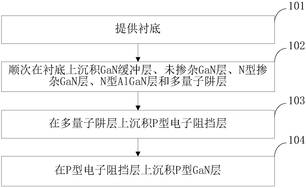
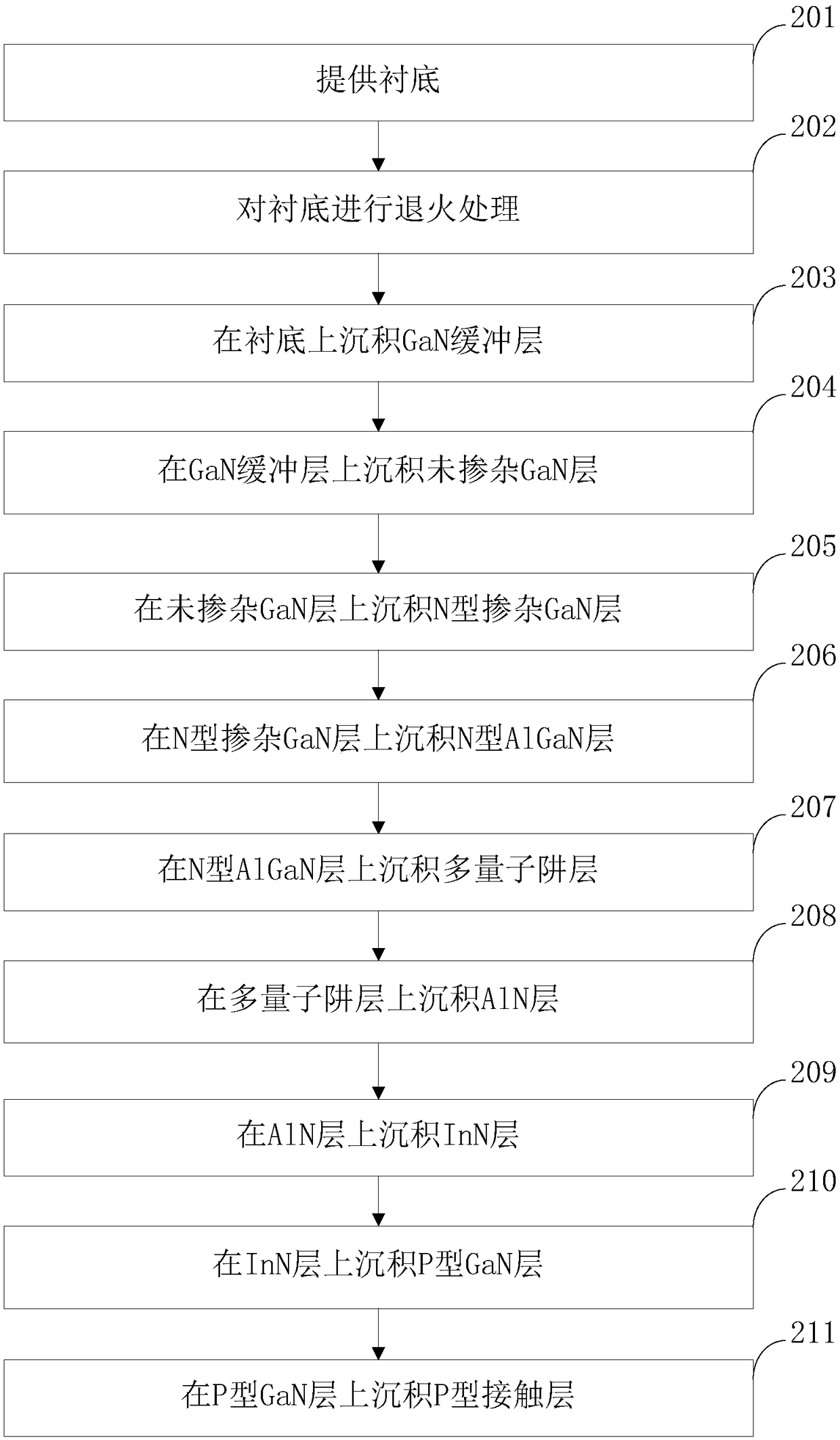
[0031] figure 1 A method for preparing a GaN-based light-emitting diode epitaxial wafer provided by an embodiment of the present invention is shown. see figure 1 , the method flow includes the following steps.

[0032] Step 101, providing a substrate.

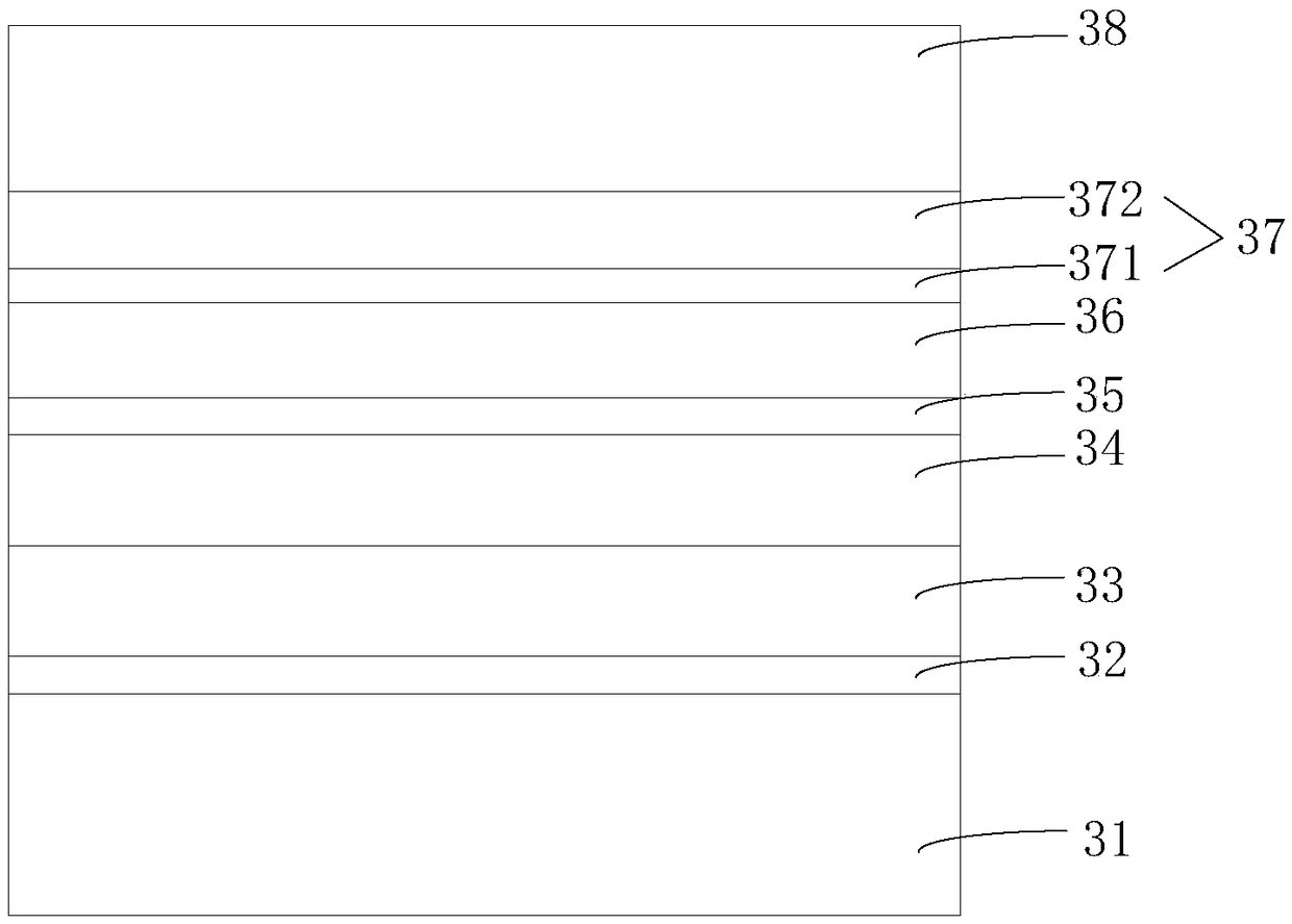
[0033] Step 102 , sequentially depositing a GaN buffer layer, an undoped GaN layer, an N-type doped GaN layer, an N-type AlGaN layer and a multiple quantum well layer on the substrate.

[0034] Embodiments of the present invention provide two structures of multiple quantum well layers.

[0035] Exemplarily, the structure of the first multi-quantum well layer is: the multi-quantum well layer includes several stacked quantum well barrier layers, and the quantum well barrier layers inc...


PUM

PropertyMeasurementUnit
Growth temperatureaaaaaaaaaa
Thicknessaaaaaaaaaa
Thicknessaaaaaaaaaa

Abstract

The invention discloses a GaN-based light-emitting diode epitaxial wafer and a manufacture method thereof, and belongs to the technical field of light-emitting diodes. The method includes providing asubstrate; sequentially depositing a GaN buffer layer, an undoped GaN layer, an N-type doped GaN layer, an N-type AlGaN layer and a multi-quantum well layer on the substrate; depositing a P-type electron blocking layer on the multi-quantum well layer, wherein the P-type electron blocking layer comprises an AlN layer and an InN layer which are sequentially stacked on the multi-quantum well layer; depositing a P-type GaN layer on the P-type electron blocking layer. The GaN-based light-emitting diode epitaxial wafer can weaken the blocking effect on holes when the electron blocking effect is strong, thereby improving the composite luminous efficiency of the electron holes in quantum wells.

Description

technical field [0001] The invention relates to the technical field of light-emitting diodes, in particular to a GaN-based light-emitting diode epitaxial wafer and a preparation method thereof. Background technique [0002] GaN (Gallium Nitride) is a typical representative of the third-generation wide-bandgap semiconductor materials. It has excellent high thermal conductivity, high temperature resistance, acid and alkali resistance, and high hardness. It is widely used in the production of blue, green, and ultraviolet led. GaN-based light emitting diodes generally include an epitaxial wafer and electrodes disposed on the epitaxial wafer. [0003] An existing epitaxial wafer of a GaN-based light-emitting diode, which includes a substrate, a buffer layer, an N-type layer, a multi-quantum well layer (also known as an active layer), and an EBL (Electron Blocking Layer) grown sequentially on the substrate. , electron blocking layer) and P-type layer. When a current flows, the ...

Claims


Application Information

Patent Timeline
IPC IPC(8): H01L33/00H01L33/14H01L33/32
CPCH01L33/0075H01L33/145H01L33/32
Inventor 曹阳郭炳磊王群乔楠张武斌吕蒙普胡加辉
Owner HC SEMITEK SUZHOU
Why Eureka
Try Eureka