Gallium nitride-based light emitting diode epitaxial wafer and preparation method thereof

A light-emitting diode, gallium nitride-based technology, applied in the direction of electrical components, circuits, semiconductor devices, etc., can solve the problems of low hole injection efficiency, small operating current, and difficult hole injection, so as to improve injection efficiency and reduce doping Miscellaneous, the effect of releasing lattice stress

Active Publication Date: 2021-10-19
HC SEMITEK ZHEJIANG CO LTD
View PDF6 Cites 0 Cited by
  • Summary
  • Abstract
  • Description
  • Claims
  • Application Information

AI Technical Summary

Problems solved by technology

However, heavy doping of Mg will introduce additional defects and impurities, making it more difficult to inject holes with low mobility, especially in micro-display LEDs, where the operating current is small and the problem of low hole injection efficiency will be more prominent.

Method used


Image

  • Gallium nitride-based light emitting diode epitaxial wafer and preparation method thereof
  • Gallium nitride-based light emitting diode epitaxial wafer and preparation method thereof
  • Gallium nitride-based light emitting diode epitaxial wafer and preparation method thereof

Examples


Embodiment Construction

[0036] In order to make the purpose, technical solution and advantages of the present disclosure clearer, the implementation manners of the present disclosure will be further described in detail below in conjunction with the accompanying drawings.

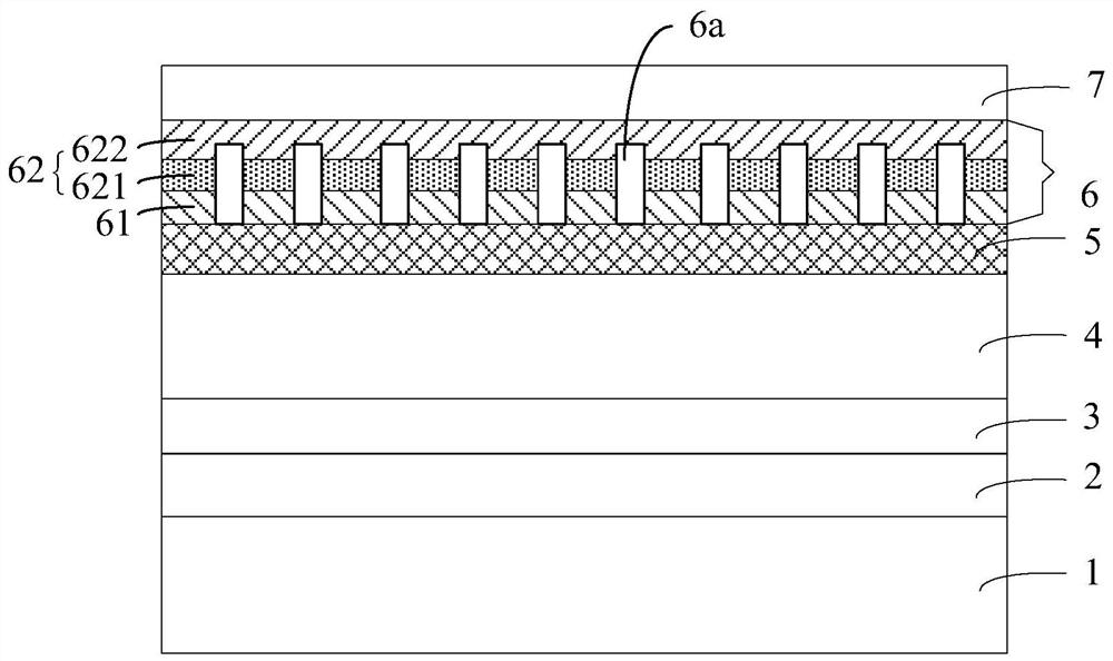
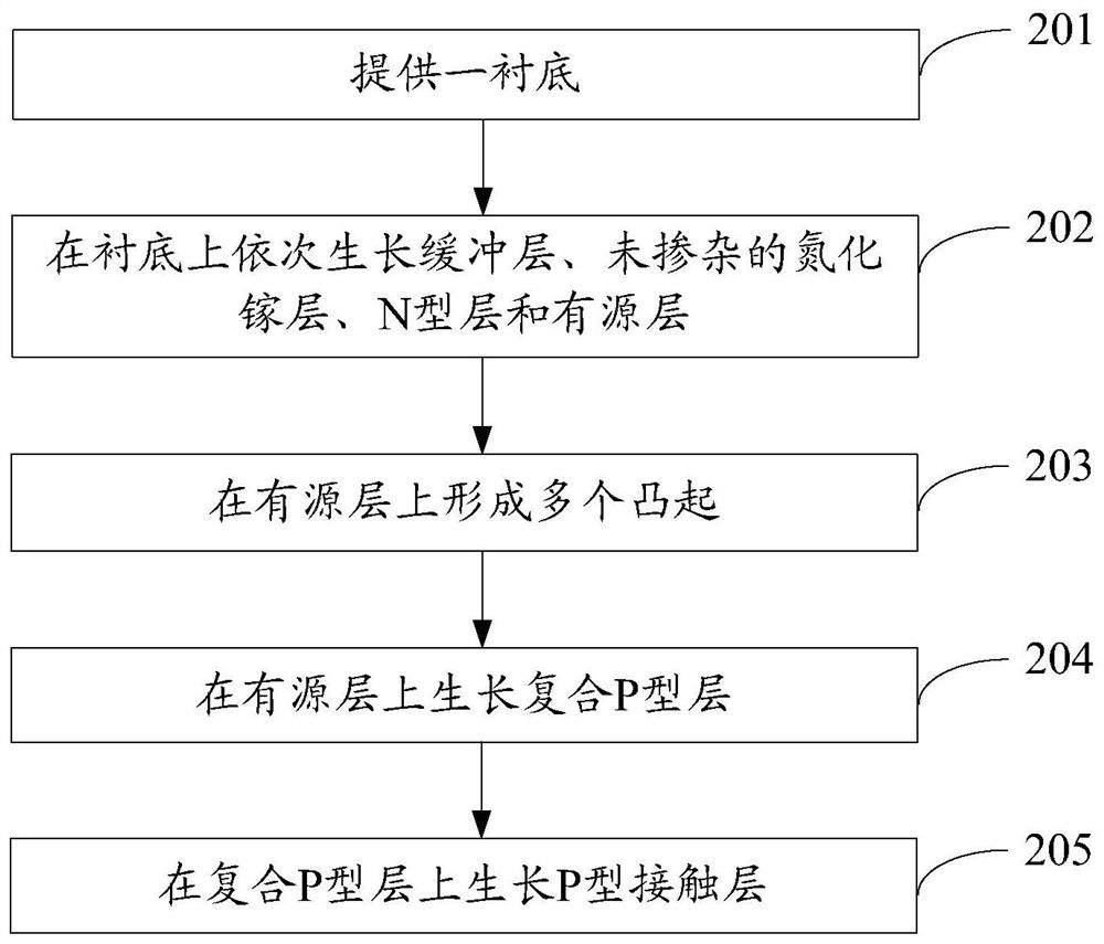
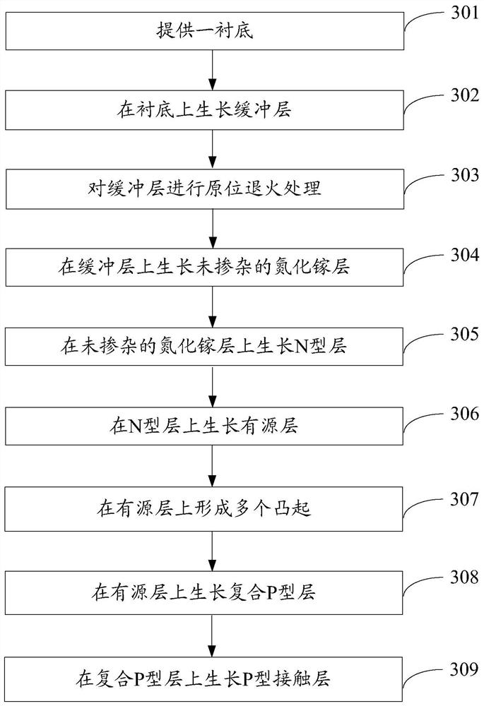
[0037] figure 1 It is a schematic structural diagram of a gallium nitride-based light-emitting diode epitaxial wafer provided by an embodiment of the present disclosure, as shown in figure 1 As shown, the light-emitting diode epitaxial wafer includes a substrate 1, a buffer layer 2, an undoped gallium nitride layer 3, an N-type layer 4, an active layer 5, and a composite P-type layer stacked on the substrate 1 in sequence. 6 and the P-type contact layer 7.

[0038] The composite P-type layer 6 includes a first composite layer 61 and a second composite layer 62 sequentially stacked on the active layer. The first compound layer 61 is a gallium nitride layer, the second compound layer 62 is a p-type gallium nitride layer, and the ac...


PUM

PropertyMeasurementUnit
heightaaaaaaaaaa
thicknessaaaaaaaaaa
thicknessaaaaaaaaaa

Abstract

The invention provides a gallium nitride-based light emitting diode epitaxial wafer and a preparation method thereof, and belongs to the technical field of semiconductors. The light emitting diode epitaxial wafer comprises a substrate, a buffer layer, an undoped gallium nitride layer, an N-type layer, an active layer, a composite P-type layer and a P-type contact layer, wherein the buffer layer, the undoped gallium nitride layer, the N-type layer, the active layer, the composite P-type layer and the P-type contact laye rare stacked on the substrate in sequence, the composite P-type layer comprises a first composite layer and a second composite layer which are stacked on the active layer in sequence, the first composite layer is a gallium nitride layer, the second composite layer is a P-type gallium nitride layer, a plurality of protrusions are arranged on the face, making contact with the first composite layer, of the active layer, and the protrusions penetrate through the first composite layer and are located in the second composite layer, the plurality of protrusions are made of gallium oxide materials. According to the light emitting diode epitaxial wafer, Mg doping can be reduced, hole expansion and effective injection under small current are improved, and the light-emitting efficiency of the epitaxial wafer is improved.

Description

technical field [0001] The disclosure relates to the technical field of semiconductors, in particular to a GaN-based light-emitting diode epitaxial wafer and a preparation method thereof. Background technique [0002] Light Emitting Diode (English: Light Emitting Diode, referred to as: LED) is a semiconductor diode that can convert electrical energy into light energy. LED has the advantages of high efficiency, energy saving, and environmental protection, and is widely used in traffic indication, outdoor full-color display and other fields. [0003] At present, gallium nitride-based LEDs have received more and more attention and research. The main body of its epitaxial structure is: substrate (sapphire substrate), gallium nitride or aluminum-doped gallium nitride buffer layer, undoped GaN layer, N Type layer, current active layer, P-type layer and P-type contact layer. Wherein, both the P-type layer and the P-type contact layer are Mg-doped GaN layers. When a current flows...

Claims


Application Information

Patent Timeline
Patent Type & Authority Applications(China)
IPC IPC(8): H01L33/24H01L33/32H01L33/00
CPCH01L33/24H01L33/32H01L33/0075H01L33/0066
Inventor 王群郭炳磊葛永晖王江波董彬忠李鹏
Owner HC SEMITEK ZHEJIANG CO LTD
Why Eureka
Try Eureka