
Eureka
For R&D, Eureka makes reading and utilizing patents & technical documents easy.
Eureka AIR
Designed for self-driven R&D workflows. Generate viable solutions, solve complex R&D challenges, empower your innovation with AI.

Eureka Materials
Designed for material experts only. Revolutionize your material R&D, from search, analyze, to developing new materials.

TechResearch
Generate reliable direction feasibility study reports for your R&D in just a few steps.

TechSeek
Discover and master advanced knowledge NOW. Basics, ideas, possibilities, all at once.

TechMind
As an expert in R&D Theories, TechMind can generates customized viable solutions instantly.

TechRisk
Analyze your overall solution with one click, know your potential R&D risks in advance.

TechMonitor
Get weekly tech updates, stay abreast of the latest tech innovations and key insights.
Photoresist removing solution and photoresist removing method
A photoresist and removal solution technology, which is applied in optics, photomechanical equipment, photosensitive material processing, etc., to achieve the effects of saving cost, improving removal effect, and improving process yield
- Summary
- Abstract
- Description
- Claims
- Application Information
AI Technical Summary
Problems solved by technology
Method used
Image

Examples
Embodiment Construction
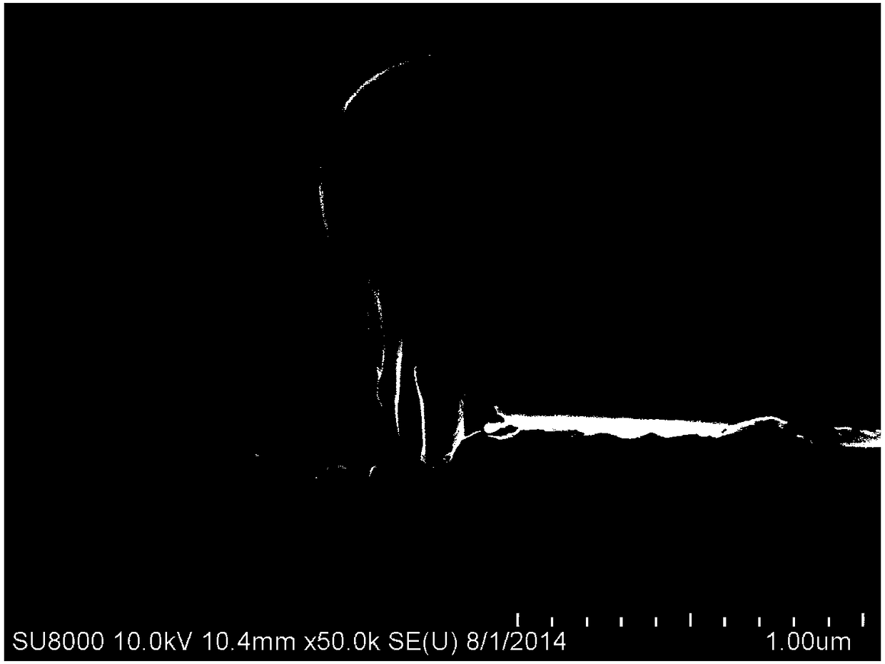
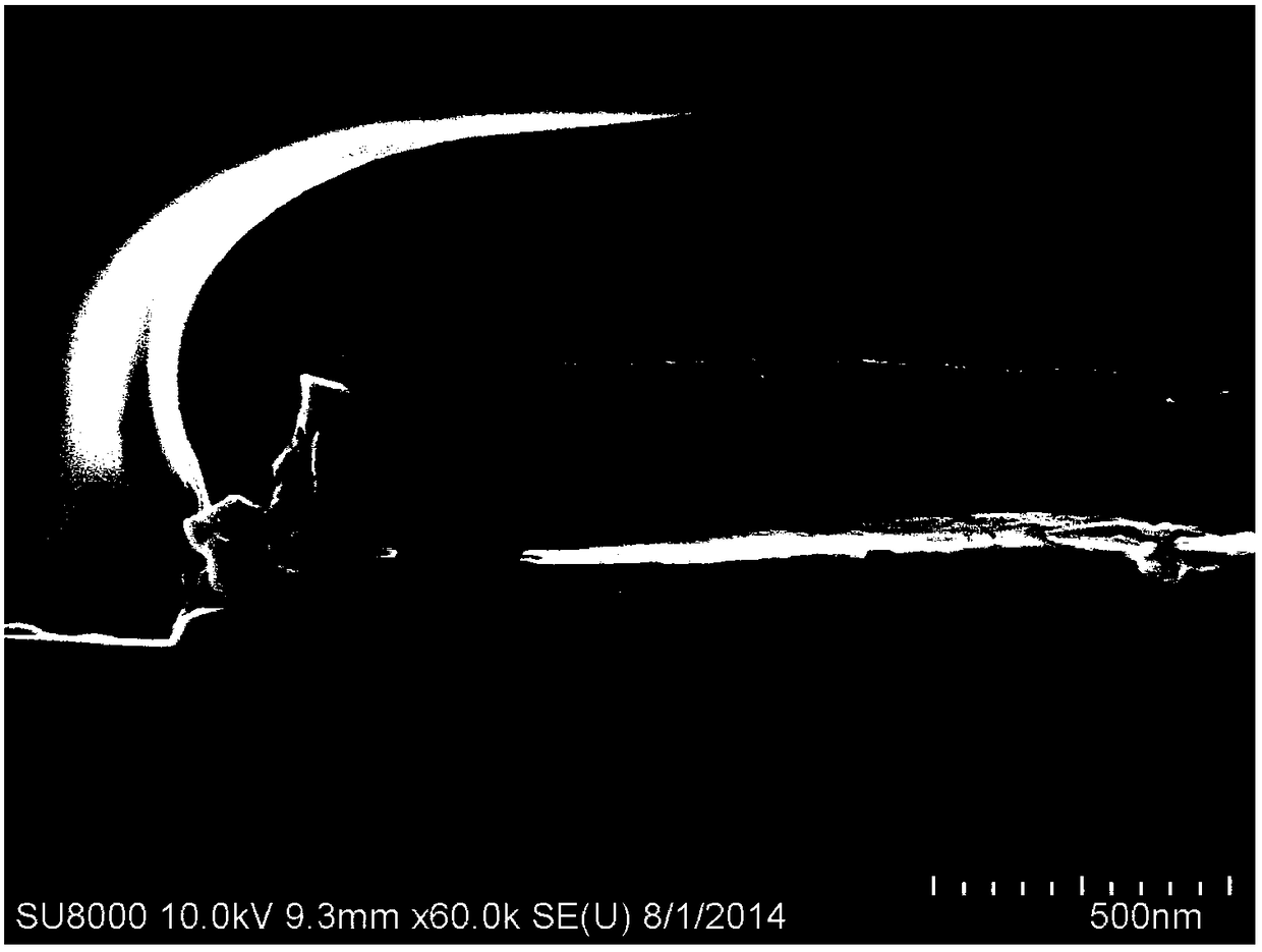
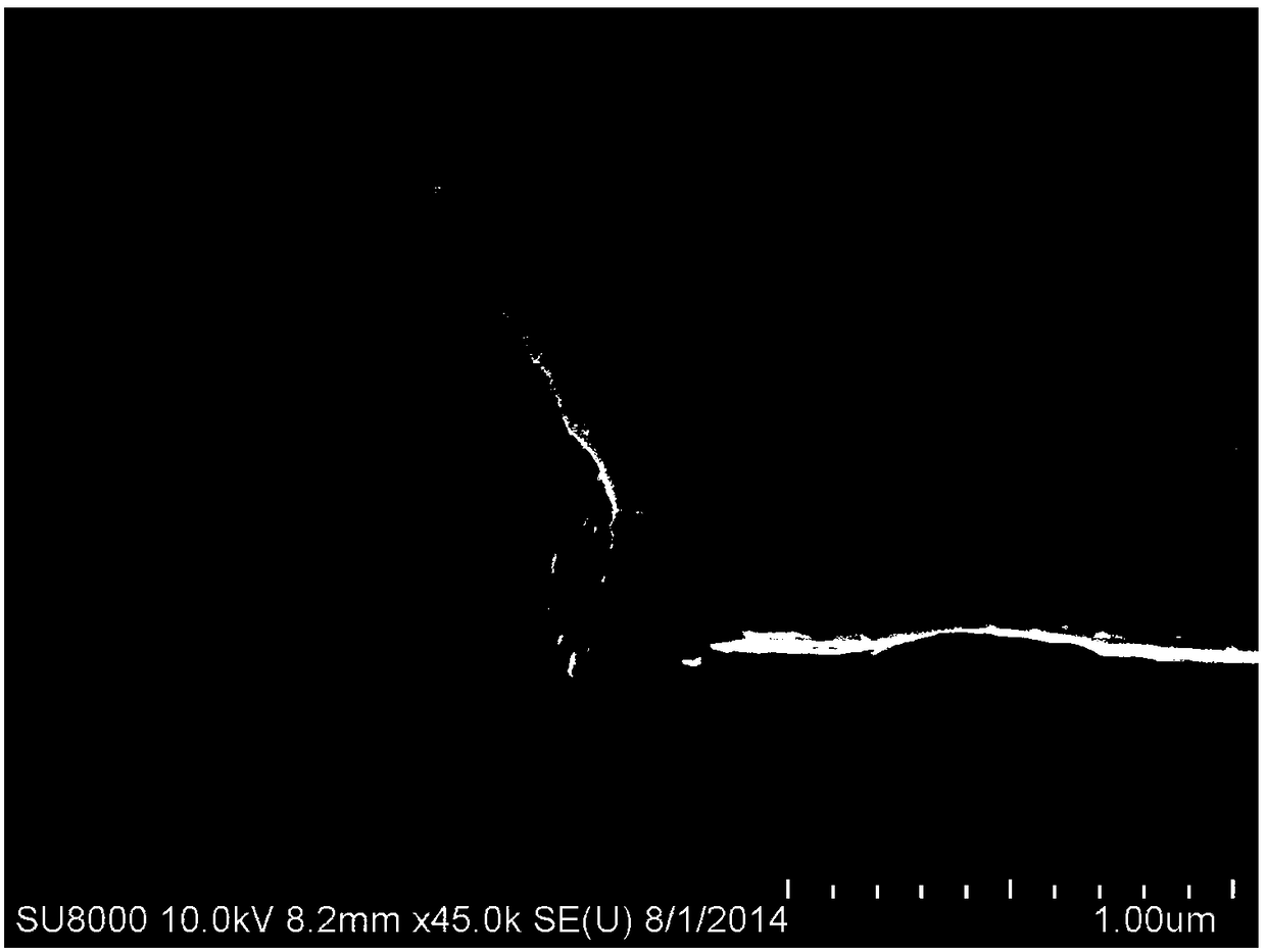
[0032] The present invention will be further described through several examples below. The following examples are just examples of the present invention, and the content of the present invention is not limited to the following examples. In the following examples, the chemical liquid used is electronic grade, wherein the mass concentration of ammonia water is 25-28%. For the convenience of calculation, in the following examples, the mass concentration of ammonia water is calculated as 28%. In the following examples, the preparation method of the test wafer used to test the removal effect is as follows: the positive photoresist (model AZ701 model AZ701) that is currently in use is coated with a thickness of 1 micron on the entire surface of the wafer using a rotating or sliding device. , AZ Electronics Materials Group (AZ Electronics Materials)), use a hot plate or an oven to perform pre-baking at a temperature of about 150°C, and then expose different wafers using photomasks wit...
PUM
 Abstract
Description
Claims
Application Information
 - R&D Engineer
- R&D Manager
- IP Professional
- Industry Leading Data Capabilities
- Powerful AI technology
- Patent DNA Extraction
Browse by: Latest US Patents, China's latest patents, Technical Efficacy Thesaurus, Application Domain, Technology Topic, Popular Technical Reports.
© 2024 PatSnap. All rights reserved.Legal|Privacy policy|Modern Slavery Act Transparency Statement|Sitemap|About US| Contact US: help@patsnap.com