QLED device with graphene oxide interfacial layer and preparation method thereof

An interfacial layer and graphene technology, which is applied in semiconductor/solid-state device manufacturing, electrical solid-state devices, semiconductor devices, etc., can solve problems such as agglomeration or settlement, uneven interface, affecting device performance and luminous uniformity, and achieve passivation Effects of interface defects, improvement of interface structure, and performance improvement of QLED devices

Active Publication Date: 2019-02-26
TCL CORPORATION
View PDF2 Cites 27 Cited by
  • Summary
  • Abstract
  • Description
  • Claims
  • Application Information

AI Technical Summary

Problems solved by technology

In the device preparation methods of the prior art, quantum dots and metal oxide nanoparticles are relatively large in size compared with ordinary ions or small organic molecules, and if ligands fall off or other reasons, they are likely to cause agglomeration or sedimentation, which greatly affects their composition. Film uniformity and film coverage
In addition, uneven quantum dot light-emitting layer or uneven metal oxide carrier transport layer will cause the interface between the two to be uneven or have a large number of defects, which greatly affects the device performance and uniformity of light emission.

Method used


Image

  • QLED device with graphene oxide interfacial layer and preparation method thereof
  • QLED device with graphene oxide interfacial layer and preparation method thereof
  • QLED device with graphene oxide interfacial layer and preparation method thereof

Examples


preparation example Construction

[0063] Based on the above-mentioned QLED device with a graphene oxide interface layer, the present invention also provides a corresponding preparation method for a QLED device with a graphene oxide interface layer, such as Image 6 As shown, it includes the following steps:

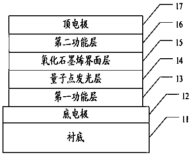
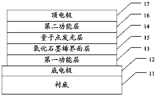
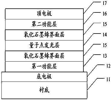
[0064] S100, depositing a bottom electrode on the substrate;

[0065] S200, sequentially depositing a first functional layer, a quantum dot light-emitting layer, and a second functional layer on the bottom electrode, wherein, between the first functional layer and the quantum dot light-emitting layer, and / or the quantum dots emit light A functionalized graphene oxide interface layer is also deposited between the layer and the second functional layer;

[0066] S300. Depositing a top electrode on the second functional layer to manufacture a QLED device with a graphene oxide interface layer.

[0067] During specific implementation, the deposition method adopted by the bottom electrode, the top electrode, a...

Embodiment 1

[0072] Spin-coat a layer of PEDOT:PSS film on the ITO conductive glass as a hole injection layer; then spin-coat a layer of TFB layer on the PEDOT:PSS layer; then spin-coat a layer of CdSe / ZnS quantum dot light-emitting layer on the TFB layer; Spin-coat a graphene oxide interface layer on the CdSe / ZnS quantum dot luminescent layer afterwards, wherein, the surface of the graphene oxide layer has a large amount of hydroxyl and carboxyl groups; spin-coat a layer on the above-mentioned graphene oxide interface layer afterwards ZnO layer; and then vapor-depositing a layer of Al cathode layer on the ZnO layer to obtain a quantum dot light-emitting diode.

Embodiment 2

[0074] Spin-coat a layer of PEDOT:PSS film on the ITO conductive glass as a hole injection layer; then spin-coat a layer of TFB layer on the PEDOT:PSS layer; then spin-coat a layer of CdSe / ZnS quantum dot light-emitting layer on the TFB layer; Then on the CdSe / ZnS quantum dot light-emitting layer, spin-coat a layer of graphene oxide interface layer, wherein, the surface of the graphene oxide layer has a large number of hydroxyl groups and mercapto groups; then spin-coat a layer of graphene oxide interface layer on the above-mentioned graphene oxide interface layer An InSnO layer; and then vapor-depositing an Al cathode layer on the InSnO layer to obtain a quantum dot light-emitting diode.


PUM


Abstract

The present invention discloses a QLED device with graphene oxide interfacial layer and a preparation method thereof. The QLED device with the graphene oxide interfacial layer includes a substrate, abottom electrode, a first functional layer, a quantum dot luminescent layer, a second functional layer, and a top electrode, wherein the substrate, the bottom electrode, the first functional layer, the quantum dot luminescent layer, the second functional layer, and the top electrode are sequentially stacked. Graphene oxide interfacial layers with functionalized functional groups are included between the first functional group and the quantum dot luminescent layer, and / or between the quantum dot luminescent layer and the second functional layer. By adding the oxide interfacial layers with functionalized functional groups between the quantum dot luminescent layer and the functional layers, the quantum dots and the nanoparticles in the functional layers can be closely anchored by electrostatic interaction or bonding, thereby effectively improving the interface structure between the luminescent layer and the functional layers, passivating interface defects, and effectively improving the performance of the QLED device.

Description

technical field [0001] The invention relates to the field of display technology, in particular to a QLED device with a graphene oxide interface layer and a preparation method thereof. Background technique [0002] Quantum dot (Quantum dot) is a quasi-zero-dimensional nanomaterial, similar to superlattice and quantum well, its particle size is about 1~100 nm, it has quantum confinement effect, surface effect, quantum size effect and quantum tunneling effect, etc. Performance, and outstanding advantages such as good monochromaticity, high color purity, narrow luminescence spectrum, etc., it is a very promising nanomaterial. Light-emitting diodes based on quantum dots are called quantum dot light-emitting diodes (Quantum dots light-emitting diode, QLED), which is a new type of display device. The advantages of quantum dot display are wide color gamut coverage, easy color control, and high color purity. It is considered to be a new star in display technology, and it is also con...

Claims


Application Information

Patent Timeline
Patent Type & Authority Applications(China)
IPC IPC(8): H01L51/50H01L51/56
CPCH10K30/865H10K50/115H10K71/00
Inventor 梁柱荣曹蔚然刘佳
Owner TCL CORPORATION
Why Eureka
Try Eureka