Deep ultraviolet semiconductor device and manufacturing method thereof

A manufacturing method and semiconductor technology, applied in the direction of semiconductor devices, electrical components, circuits, etc., can solve the problems of low P-type doping efficiency, low efficiency of ultraviolet LED, low efficiency, etc., to reduce the turn-on voltage, reduce the barrier barrier, The effect of lowering the resistivity

Inactive Publication Date: 2019-03-05
SUZHOU INST OF NANO TECH & NANO BIONICS CHINESE ACEDEMY OF SCI +1
View PDF3 Cites 7 Cited by
  • Summary
  • Abstract
  • Description
  • Claims
  • Application Information

AI Technical Summary

Problems solved by technology

However, compared with LEDs in other wavelength bands, the efficiency of ultraviolet LEDs is relatively low, especially the external quantum efficiency of deep ultraviolet LEDs with a wavelength of less than 360nm is mostly lower than 10%.
[0003] At present, the main reasons for the low efficiency of deep ultraviolet LEDs are: the quality of epitaxially grown AlGaN cry

Method used


Image

  • Deep ultraviolet semiconductor device and manufacturing method thereof
  • Deep ultraviolet semiconductor device and manufacturing method thereof
  • Deep ultraviolet semiconductor device and manufacturing method thereof

Examples


Example Embodiment

[0026] In view of the deficiencies in the prior art, the inventor of this case was able to propose the technical solution of the present invention after long-term research and extensive practice. The technical solution, its implementation process and principle will be further explained as follows. However, it should be understood that within the scope of the present invention, each technical feature of the present invention and each technical feature specifically described in the following (such as an embodiment) can be combined with each other to form a new or preferred technical solution. Due to space limitations, we will not repeat them here.

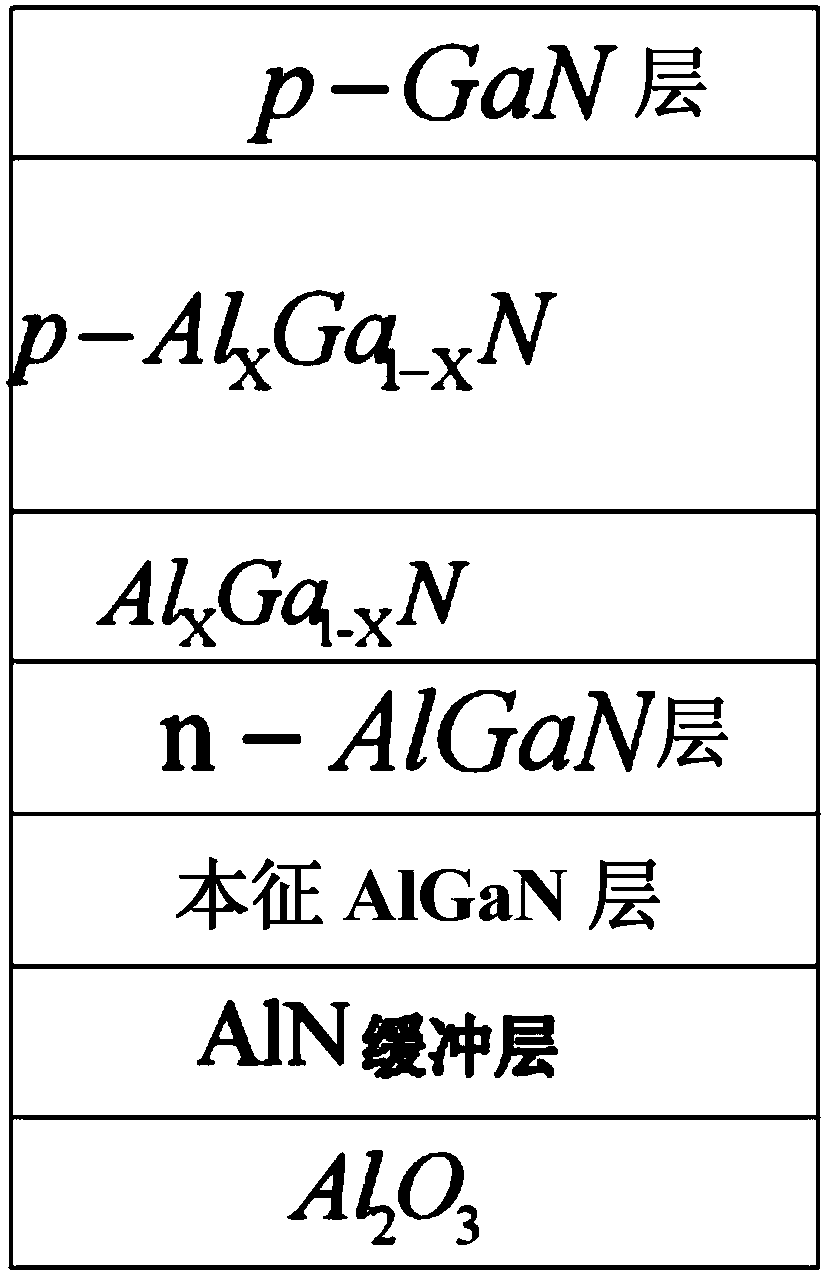
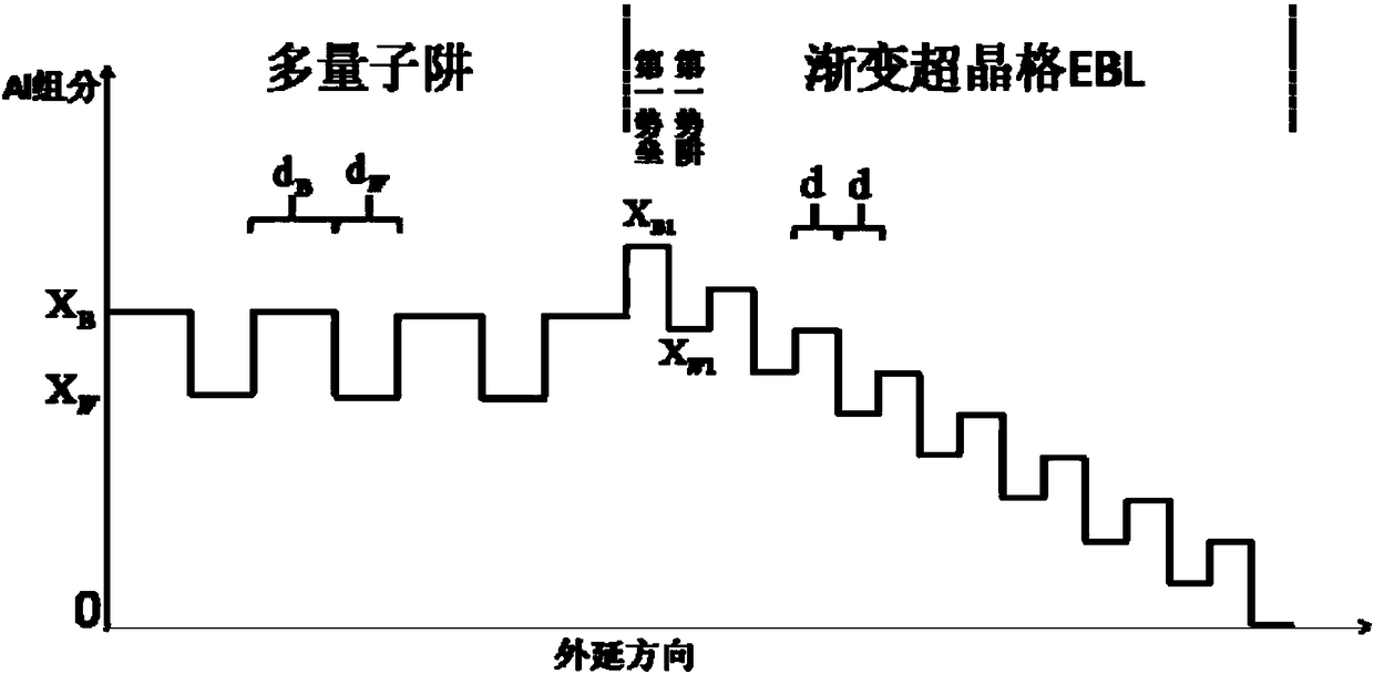
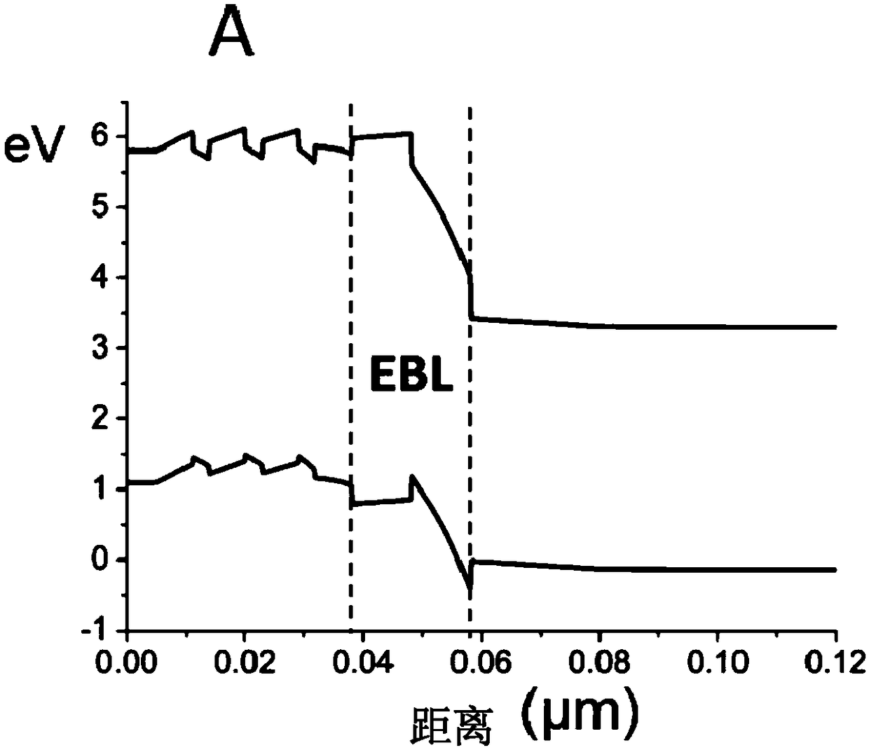
[0027] One aspect of the embodiments of the present invention provides a deep ultraviolet semiconductor device, including an n-type AlGaN layer, a multi-quantum well structure (MQW), an electron blocking layer (EBL) and a p-type GaN layer arranged in sequence along a set direction, so that The electron blocking layer comprises p-typ...


PUM

PropertyMeasurementUnit
Thicknessaaaaaaaaaa
Thicknessaaaaaaaaaa
Thicknessaaaaaaaaaa

Abstract

The invention discloses a deep ultraviolet semiconductor device and a manufacturing method thereof. The deep ultraviolet semiconductor device comprises an n-type AlGaN layer, a multi-quantum-well structure, an electron blocking layer and a p-type GaN layer which are arranged in sequence along a set direction, wherein the electron blocking layer comprises a p-type AlxGa1-xN with a gradient super-lattice structure, wherein x is greater than or equal to 0 and less than 1; the gradient super-lattice structure comprises a plurality of super-lattice barrier layers and a plurality of super-lattice potential well layers which are alternately stacked; in the selected direction, the contents of Al component from the first super-lattice barrier layer to the last super-lattice barrier layer are gradually decreased to be zero, and the contents of Al component from the first super-lattice potential well layer to the last super-lattice potential well layer are gradually decreased to be zero. By virtue of the gradient super-lattice structure, an energy band can be modulated, so that the problem that the P-type doping efficiency is low due to high activation energy is relieved, electrons are effectively limited in the quantum well, the blocking potential barrier injected by the holes to the quantum well is reduced, and the performance of the deep ultraviolet LED device is improved.

Description

technical field [0001] The invention relates to a semiconductor device, in particular to a deep ultraviolet semiconductor device based on a graded superlattice structure electron blocking layer and a manufacturing method thereof, belonging to the technical field of semiconductor devices. Background technique [0002] Ultraviolet LEDs based on AlGaN materials have different application fields according to different wavelengths and powers, such as: medical treatment, photolithography, purification, anti-counterfeiting, detection, etc. Compared with traditional mercury light sources, AlGaN-based ultraviolet LEDs have the advantages of energy saving, environmental protection, low working voltage, and long working life. However, compared with LEDs in other wavelength bands, the efficiency of ultraviolet LEDs is relatively low, especially the external quantum efficiency of deep ultraviolet LEDs with a wavelength of less than 360nm is mostly lower than 10%. [0003] At present, th...

Claims


Application Information

Patent Timeline
IPC IPC(8): H01L33/14H01L33/04H01L33/00
CPCH01L33/04H01L33/0066H01L33/0075H01L33/145
Inventor 陈刚张纪才王建峰徐科
Owner SUZHOU INST OF NANO TECH & NANO BIONICS CHINESE ACEDEMY OF SCI
Why Eureka
Try Eureka