Circuit board with electromagnetic shielding function, and manufacturing method of circuit board

A technology of electromagnetic shielding and manufacturing method, applied in printed circuit manufacturing, printed circuit, printed circuit components and other directions, can solve the problems of poor shielding effect, complicated circuit board manufacturing, easy to produce gaps, etc., so as to reduce the manufacturing process and improve electromagnetic shielding. Effect, simple effect of production process

Active Publication Date: 2019-03-05
HONGQISHENG PRECISION ELECTRONICS (QINHUANGDAO) CO LTD +1
View PDF15 Cites 3 Cited by
  • Summary
  • Abstract
  • Description
  • Claims
  • Application Information

AI Technical Summary

Problems solved by technology

[0004] However, the circuit board with an electromagnetic shielding film attached to the outer layer of the circuit board to prevent electromagnetic radiation is complicated and thick.
[0005] On the outer layer of the circuit board, an aluminu

Method used


Image

  • Circuit board with electromagnetic shielding function, and manufacturing method of circuit board
  • Circuit board with electromagnetic shielding function, and manufacturing method of circuit board
  • Circuit board with electromagnetic shielding function, and manufacturing method of circuit board

Examples


Embodiment Construction

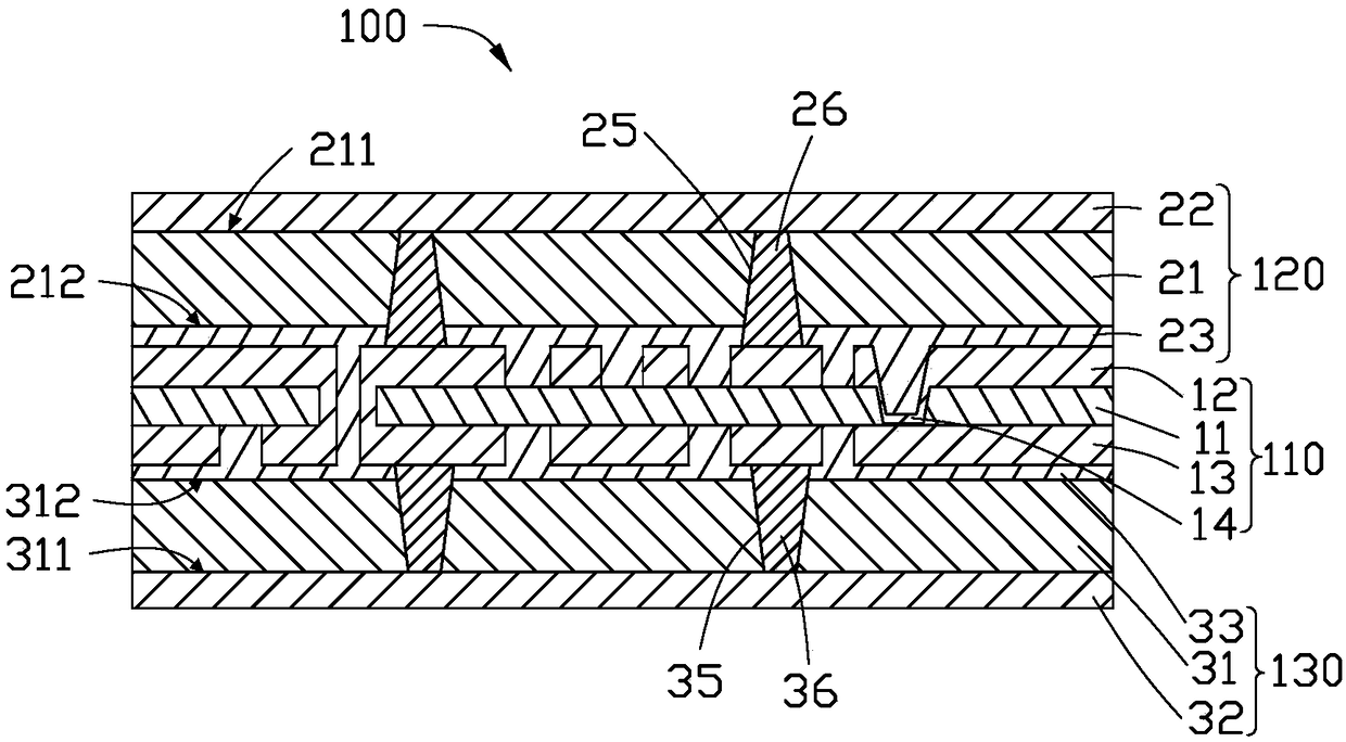
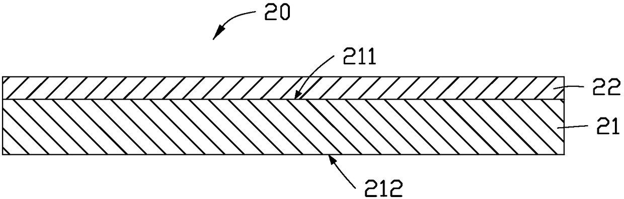
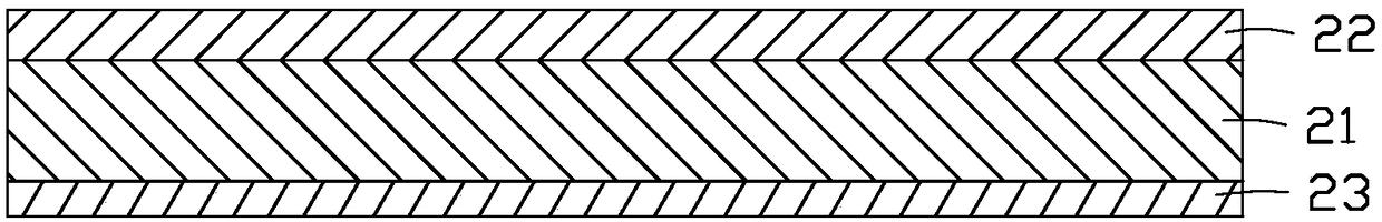
[0029] In order to further illustrate the technical means and effects that the present invention takes to reach the intended purpose of the invention, the following in conjunction with the appended Figure 1-7 And the preferred implementation mode, the specific implementation, structure, characteristics and effects of the circuit board with electromagnetic shielding function and its manufacturing method provided by the present invention are described in detail as follows.

[0030] The orientation words "first", "second", "third", and "fourth" used herein are all defined by the positions of the first substrate and the second substrate when used, and do not limit .

[0031] Unless otherwise defined, all technical and scientific terms used herein have the same meaning as commonly understood by one of ordinary skill in the technical field of the invention. The terminology used herein in the description of the present invention is only for the purpose of describing specific embodi...


PUM


Abstract

Disclosed is a manufacturing method of a circuit board with an electromagnetic shielding function. The manufacturing method comprises the following steps that a single-sided copper-clad substrate is provided, wherein the single-sided copper-clad substrate comprises a first base material layer and a first copper foil layer; the first base material layer comprises a first surface and a second surface opposite to the first surface, and the first copper foil layer is formed on the first surface; a first low-loss dielectric layer is formed on the second surface; at least one first containing hole which penetrates through the first low-loss dielectric layer and the first base material layer is formed, and a first conductive paste is filled in the first containing hole, so as to form a first electromagnetic shielding layer; and a circuit substrate is provided, and the first electromagnetic shielding layer is pressed on the circuit substrate, wherein the circuit substrate comprises a first conductive circuit layer, and the first conductive paste is directly electrically connected with the first conductive circuit layer and the first copper foil layer. The invention further relates to the circuit board with the electromagnetic shielding function.

Description

technical field [0001] The invention relates to the field of electromagnetic shielding manufacturing, in particular to a circuit board with electromagnetic shielding function and a manufacturing method thereof. Background technique [0002] When common electronic equipment is working, because of the intermittent or continuous change of the working voltage and current, the internal electronic components will often cause electromagnetic radiation energy of a certain frequency, which will radiate to the surrounding environment and cause damage to the adjacent electronic components. interference, or even cause the adjacent electronic components to fail to work properly. Moreover, as mid-to-high-end consumer electronics products have higher quality requirements, their requirements for electromagnetic shielding are also getting higher and higher. [0003] Common electronic equipment implements electromagnetic shielding by adding a shielding cover locally on the circuit board. Spe...

Claims


Application Information

Patent Timeline
IPC IPC(8): H05K1/02H05K3/10
CPCH05K1/0227H05K3/107
Inventor 叶子建
Owner HONGQISHENG PRECISION ELECTRONICS (QINHUANGDAO) CO LTD
Why Eureka
Try Eureka