Femtosecond laser manufacturing method for tunable phase change nanostructure super surfaces

A femtosecond laser and nanostructure technology, applied in the field of femtosecond laser applications, can solve problems such as complex processes and achieve simple and precise results

Active Publication Date: 2019-03-08
BEIJING UNIV OF TECH
View PDF6 Cites 7 Cited by
  • Summary
  • Abstract
  • Description
  • Claims
  • Application Information

AI Technical Summary

Problems solved by technology

[0004] The purpose of the present invention is to solve the problems of complex process, precise, efficient, ordered and large-area processing of nanostructure units in the current supersurface nanostructure processing process, and provide a femtosecond laser-induced phase change material to realize tunable phase change nanostructures Methods of Fabrication of Metasurfaces

Method used


Image

  • Femtosecond laser manufacturing method for tunable phase change nanostructure super surfaces
  • Femtosecond laser manufacturing method for tunable phase change nanostructure super surfaces
  • Femtosecond laser manufacturing method for tunable phase change nanostructure super surfaces

Examples


specific Embodiment 1

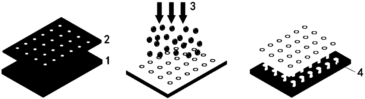
[0032] For amorphous columnar Ge 2 Sb 2 Te 5 Taking nanostructures for femtosecond laser morphology control as an example, the specific processing steps are as follows:

[0033] (1) Sample preparation: In this example, 40nm thick Ge was plated on a 10mm×10mm×1mm silicon dioxide substrate by magnetron sputtering. 2 Sb 2 Te 5 film, and then remove the AAO template to obtain columnar nanostructures;

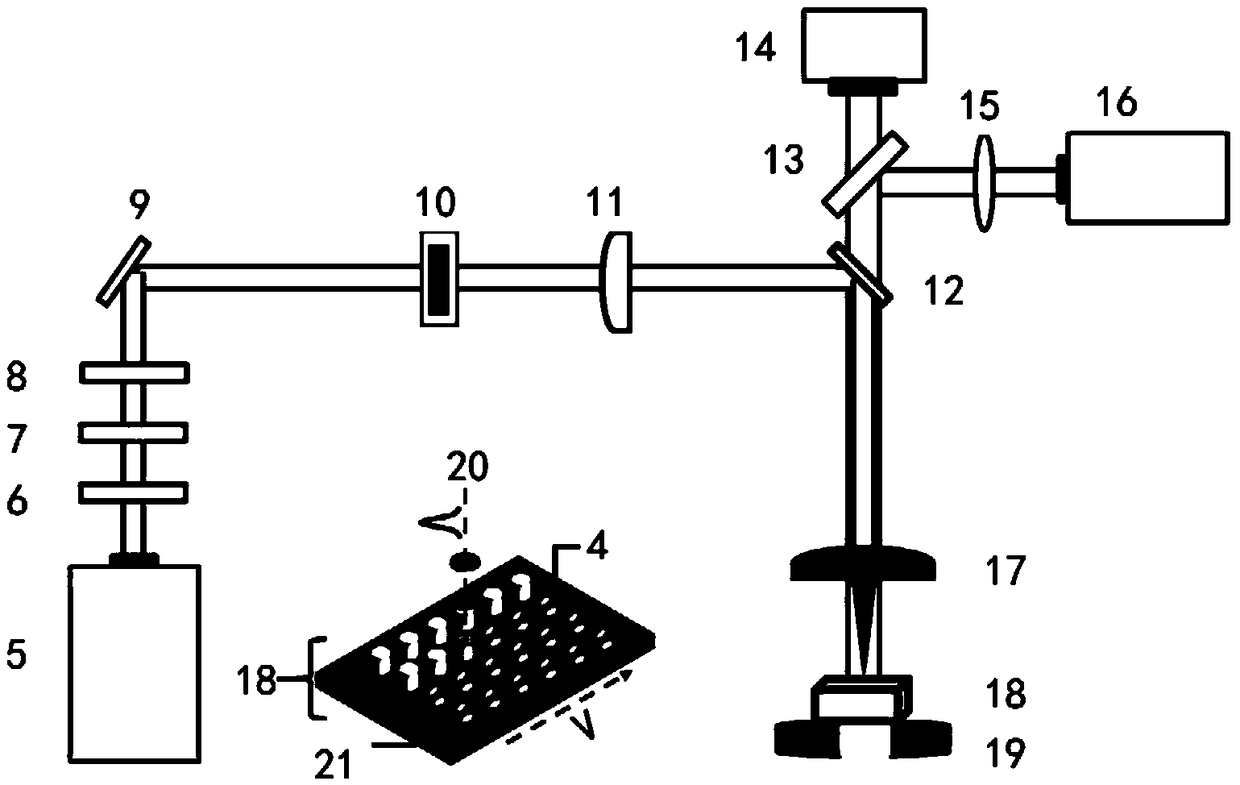
[0034] (2) The processed sample 18 is fixed on the six-dimensional mobile platform 19, and the femtosecond laser pulse is focused by a double-glued achromatic plano-convex lens 17 with a focal length of 100 mm, so that the circular Gaussian beam can act on the surface of the processed sample 18 , through the observation of the imaging CCD16, adjust the optical path so that the incident laser light is perpendicular to the surface of the sample 18;

[0035] (3) Utilize the combination of the half-wave plate 6 and the polarizer 7 and the continuous attenuation plate 8 to adjust t...

specific Embodiment 2

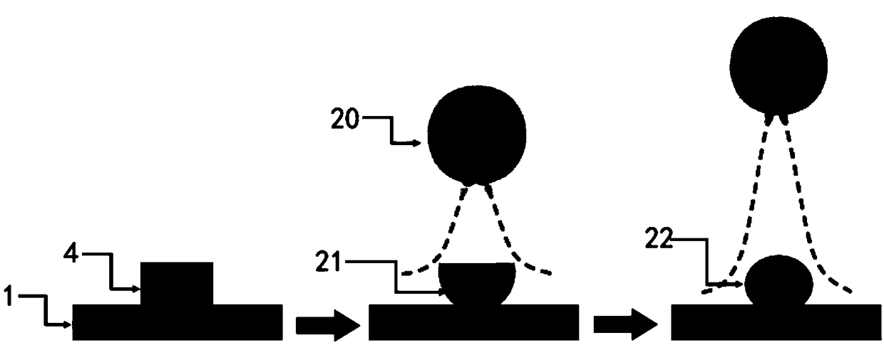
[0039] With the spherical Ge of the crystalline state that utilizes example one to make 2 Sb 2 Te 5 The nanostructure is used as a sample, and the control of femtosecond induced phase transition is taken as an example. The specific processing steps are as follows:

[0040] (1) Adjust the optical path: add a plano-convex cylindrical mirror 11 between the dichroic mirror 12 and the mechanical switch 10, use beam shaping to focus the beam line, and rotate the cylindrical mirror to make the long axis direction of the spot coincide with the translation stage Y Axis parallel;

[0041] (2) repeat the process (2) in the specific embodiment one;

[0042] (3) Utilize the combination of the half-wave plate 6 and the polarizer 7 and the continuous attenuation plate 8 to adjust the laser energy, so that the laser single pulse energy changes continuously from small to large between 0.5-1.1 times the ablation threshold;

[0043] (4) Using a single pulse to irradiate the surface of the sa...


PUM


Abstract

The invention relates to a femtosecond laser manufacturing method for tunable phase change nanostructure super surfaces, and belongs to the technical field of femtosecond laser application. The femtosecond laser manufacturing method aims to solve the problem that in the current super-surface nanostructure processing process, the technology is complicated, and the shortcomings of accurate, efficient, orderly and large-area processing of nano structure units exist are solved. According to a femtosecond laser manufacturing method, the expected morphology of the nano structure is prepared in accurate, efficient, orderly and large-scope manner with the relatively-simple technology, instantaneous electronic excitation dynamics during action of femtosecond laser and phase-change material surfacesare regulated, modulation of the distance, the morphology, the phase state and the arranging manner of the nano structure units of the phase-change material super surfaces and large-format manufacturing and modification are achieved. Critical application values are achieved in the aspects of gradient super-surfaces, information storage, holographic imaging, electromagnetic wave manipulation, switchable or reconfigurable components and the like.

Description

technical field [0001] The invention relates to a method for realizing a tunable phase-change nanostructure metasurface by using a femtosecond laser-induced phase-change material, and belongs to the technical field of femtosecond laser application. Background technique [0002] In recent years, metasurfaces have become a rapidly developing field of research because of their superior manipulation of light and their many functions in ultrathin optical applications. Compared with metamaterials, metasurfaces have attracted extensive attention from researchers due to their advantages such as low profile, low loss, and easy design and implementation. Based on its passive electromagnetic properties, such as negative refractive index or perfect absorption, a large number of functional devices based on nanostructured metasurfaces have emerged, which have a wide range of applications in the fields of biomedicine, biosensing, chemical catalysis, solar cells, and nano-optoelectronics. ...

Claims


Application Information

Patent Timeline
IPC IPC(8): B23K26/36C23C14/35C23C14/04C23C14/58
CPCB23K26/36C23C14/042C23C14/35C23C14/5873
Inventor 韩伟娜李东方袁艳萍陈继民刘富荣
Owner BEIJING UNIV OF TECH
Why Eureka
Try Eureka