CMOS technology multi-frequency metamaterial absorption structure based terahertz microbolometer

A microbolometer and absorption structure technology, applied in the field of terahertz microbolometers, can solve the problems of being susceptible to environmental interference, low resolution, and low detection probability, etc.

Inactive Publication Date: 2019-03-08
TIANJIN UNIV
View PDF3 Cites 2 Cited by
  • Summary
  • Abstract
  • Description
  • Claims
  • Application Information

AI Technical Summary

Problems solved by technology

[0005] At present, terahertz single-frequency detectors generally have problems such as low detection probability, low resolution, and susceptibility to environmental interference, which reflects the necessity of multi-frequency detectors

Method used


Image

  • CMOS technology multi-frequency metamaterial absorption structure based terahertz microbolometer
  • CMOS technology multi-frequency metamaterial absorption structure based terahertz microbolometer
  • CMOS technology multi-frequency metamaterial absorption structure based terahertz microbolometer

Examples


specific example

[0036] A specific example is given as follows:

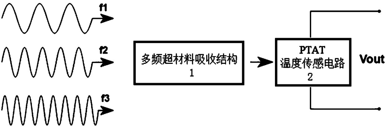
[0037] This example presents a triple-frequency terahertz metamaterial absorption structure based on a 55nm CMOS process with operating frequencies of 910GHz, 2.58THz and 4.3THz, and combined with a PTAT temperature sensing circuit to form a room temperature terahertz microbolometer.

[0038] 1. Terahertz microbolometer based on 55nm CMOS process tri-frequency metamaterial absorber including absorption structure and temperature sensor circuit;

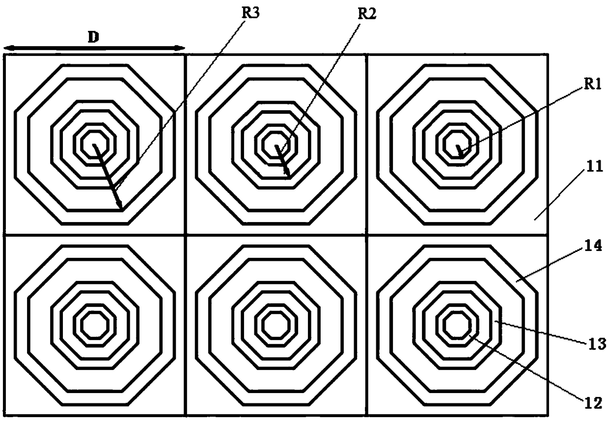
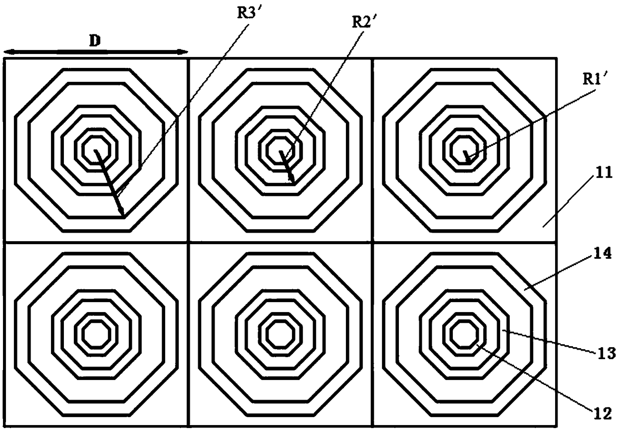
[0039] 2. The first part is the design of the three-band metamaterial absorption structure. The specific plan is to use the material properties and size parameters of the 55nm CMOS process to design and model the three-band metamaterial absorption structure in HFSS software, and propose a three-band metamaterial absorption structure. A periodic metamaterial absorption structure composed of two double-layer regular octagonal resonant rings. The OI and EA metal layers in the application p...


PUM


Abstract

The invention discloses a CMOS technology multi-frequency metamaterial absorption structure based terahertz microbolometer. The terahertz microbolometer includes a silicon substrate made by adopting astandard 55nmCMOS technology; the silicon substrate is provided with a multi-frequency metamaterial absorption structure which can simultaneously receive electromagnetic waves in three frequency bands, and a PTAT temperature sensing circuit which can receiving the output signal of the multi-frequency metamaterial absorption structure; and the output end of the PTAT temperature sensing circuit canform the output end of the terahertz microbolometer. To form the terahertz microbolometer by combining the CMOS technology based multi-frequency metamaterial absorption structure with the novel PTATtemperature sensing circuit is realized for the first time; the multi-frequency metamaterial absorption structure can be used to receive the electromagnetic waves with different frequencies so that electromagnetic energy can be converted into heat; and the heat can be converted into an output electric signal through the PTAT temperature sensing circuit, so that the simultaneous detection of terahertz signals in three frequency bands which are 910 GHz, 2.58 THz and 4.3 THz can be realized, and therefore, an effective method for multi-frequency terahertz heat detection can be obtained.

Description

technical field [0001] The invention relates to a room temperature microbolometer. In particular, it relates to a terahertz microbolometer based on a CMOS process multi-frequency metamaterial absorption structure. Background technique [0002] Terahertz wave is an electromagnetic wave with a frequency range between 0.1THz and 10THz. It is located between infrared and microwave in the electromagnetic spectrum. It has many superior characteristics, mainly as follows: (1) It has low energy and penetrates objects It is not easy to ionize and does not cause harm to the human body; (2) After many chemical substances are irradiated by terahertz waves, they resonate with terahertz waves, which can screen special chemical substances; (3) Terahertz imaging has strong penetrating ability, It can penetrate common packaging materials and "see" dangerous items such as knives and guns; (4) In the terahertz frequency band, a lot of information that is hidden and not fully utilized by human...

Claims


Application Information

Patent Timeline
Patent Type & Authority Applications(China)
IPC IPC(8): G01J5/20
CPCG01J5/20G01J2005/204
Inventor 马建国王旭傅海鹏马凯学
Owner TIANJIN UNIV
Why Eureka
Try Eureka