Gallium oxide semiconductor Schottky diode and manufacturing method thereof

A technology of Schottky diodes and fabrication methods, which are applied in semiconductor/solid-state device manufacturing, semiconductor devices, electrical components, etc., can solve the problems of unfavorable industrial production, device performance degradation, and high fabrication costs, achieve excellent device performance, and reduce interface Density of states and excellent performance

Pending Publication Date: 2019-03-08
SHANDONG UNIV
View PDF0 Cites 5 Cited by
  • Summary
  • Abstract
  • Description
  • Claims
  • Application Information

AI Technical Summary

Problems solved by technology

[0004] As mentioned earlier, most of the Ga 2 o 3 The reports of SBDs all use inert metals as Schottky anodes, whic

Method used


Image

  • Gallium oxide semiconductor Schottky diode and manufacturing method thereof
  • Gallium oxide semiconductor Schottky diode and manufacturing method thereof
  • Gallium oxide semiconductor Schottky diode and manufacturing method thereof

Examples


Embodiment Construction

[0033] The present invention will be further described below in conjunction with the accompanying drawings and embodiments.

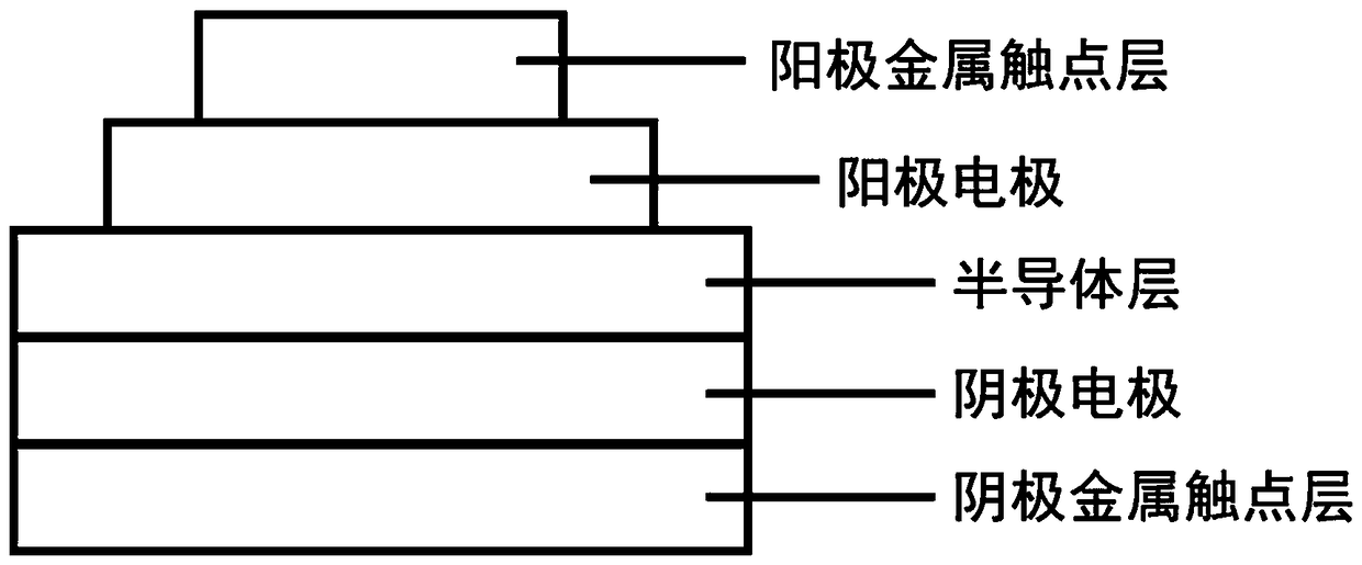
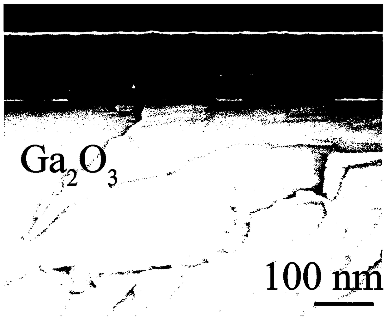
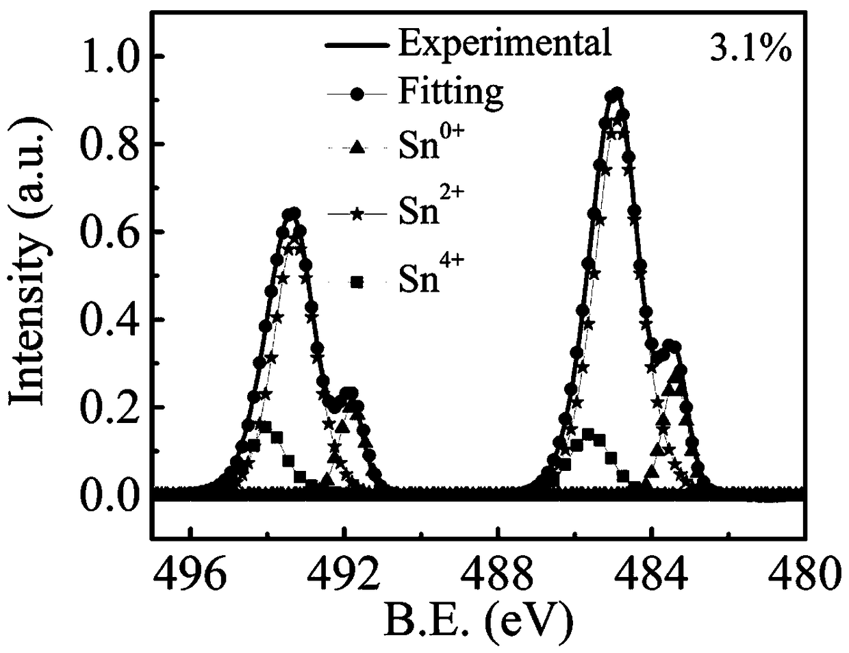
[0034] Such as figure 1 As shown, a schematic diagram of the structure of the gallium oxide semiconductor Schottky diode of the present invention is provided, which is composed of a semiconductor layer, an anode electrode, an anode metal contact layer, a cathode electrode, and a cathode metal contact layer. The anode electrode and the cathode electrode are respectively It is arranged on two surfaces of the semiconductor layer, and forms Schottky contact and ohmic contact with the semiconductor layer respectively. The semiconductor layer is made from Ga 2 o 3 Ga with a thickness of 30-600 μm removed from the crystal 2 o 3 Thin sheet, the anode electrode adopts tin oxide SnO with a thickness of 20-200nm x film, thus forming a Ga with excellent performance 2 o 3 Semiconductor Schottky diodes. The outer surface of the anode electrode is provided wit...


PUM

PropertyMeasurementUnit
Carrier concentrationaaaaaaaaaa
Thicknessaaaaaaaaaa
Thicknessaaaaaaaaaa

Abstract

The invention discloses a gallium oxide (Ga2O3) semiconductor Schottky diode. The Ga2O3 semiconductor Schottky diode comprises a semiconductor layer, an anode electrode and a cathode electrode; the semiconductor layer is Ga2O3 film, the anode electrode is oxide of stannum (SnOx). The manufacturing method of the Schottky diode disclosed by the invention comprises the following steps: a) preparing aGa2O3 sheet; b) cleaning the sheet; c) etching the Ga2O3 sheet; d) preparing cathode and metal contact point layer; e) performing annealing treatment; f) preparing the SnOx film; and g) preparing ananode metal contact point layer. An ideal factor of the Ga2O3 semiconductor Schottky diode is 1.02 and extremely close to 1, the barrier height is 1.17eV, and the switch ratio exceeds 1010; and the acquired Schottky diode is excellent in performance. Through the manufacturing method of the Schottky diode disclosed by the invention, the SnOx is used as the Schottky contact electrode, and then the high-performance Ga2O3 Schottky diode is obtained.

Description

technical field [0001] The present invention relates to a kind of gallium oxide semiconductor schottky diode and its manufacturing method, more specifically, relate to a kind of oxide (SnO x ) a gallium oxide semiconductor Schottky diode as a Schottky anode and a manufacturing method thereof. Background technique [0002] As the basic components in semiconductor circuits, Schottky barrier diodes (SBDs) have great applications in radio frequency identification tags, solar cells, amplifiers, photodetectors and logic gates. High-performance Xiao The terky diode plays a vital role. High-performance Schottky diodes can also be used in large-array RRAMs and phase-change memories to reduce parasitic currents. Gallium oxide (Ga 2 o 3 ), as a wide bandgap metal oxide semiconductor, has become a research hotspot in electronics and optoelectronics due to its wide bandgap of 4.5-4.9 eV and large breakdown field strength of 6-8 MV / cm. Large size and high quality Ga 2 o 3 Single cr...

Claims


Application Information

Patent Timeline
IPC IPC(8): H01L29/872H01L29/24H01L29/47H01L21/34
CPCH01L29/24H01L29/47H01L29/66969H01L29/872Y02P70/50
Inventor 辛倩杜路路徐明升宋爱民
Owner SHANDONG UNIV
Why Eureka
Try Eureka