A silicon-based photoelectric material and its preparation method
A photoelectric material and silicon-based technology, which is applied in the manufacture of circuits, electrical components, semiconductors/solid-state devices, etc., can solve the problems of low luminous efficiency and achieve the effects of improved luminous performance, increased luminous peak intensity, and improved luminous efficiency
- Summary
- Abstract
- Description
- Claims
- Application Information
AI Technical Summary
Problems solved by technology
Method used
Image


Examples
preparation example Construction
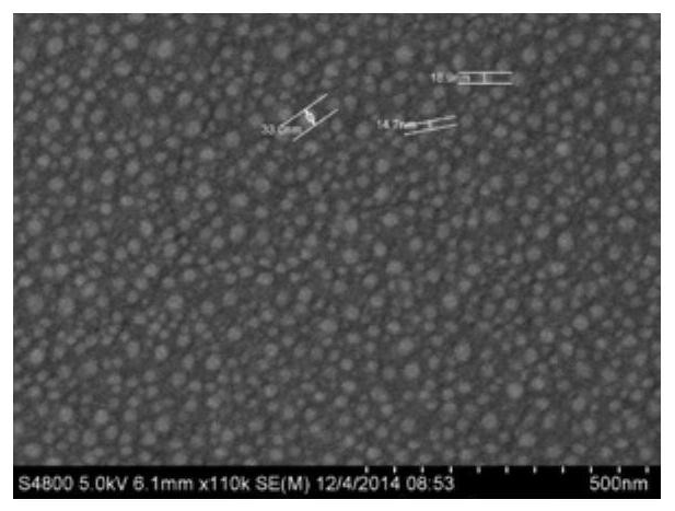
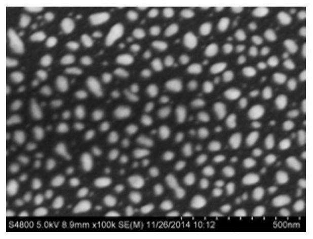
[0025]An embodiment of the present invention provides a method for preparing a silicon-based optoelectronic material, including: obtaining a clean monocrystalline silicon wafer; preparing Er-doped CeO on the surface of the monocrystalline silicon wafer2Thin film, to obtain silicon-based Er-doped CeO2Thin film; CeO doped in the Er2Prepare Ag film on the surface of the film to obtain Er-doped CeO on silicon2Thin film Ag film; doping the silicon-based Er with CeO2The thin-film Ag film is heat-treated under the protection of Ar gas, so that the Ag film is formed into an Ag particle layer, thereby obtaining a silicon-based photoelectric material.
[0026]As follows, the preparation method of the silicon-based optoelectronic material provided by the embodiment of the present invention will be described in detail through the examples.
Embodiment 1
[0028]Perform RCA standard cleaning on monocrystalline silicon wafers;
[0029]Rinse the cleaned monocrystalline silicon wafer with a HF solution of HF: water=1:4 to obtain a clean monocrystalline silicon wafer;
[0030]Preparation of 150nm thick Er-doped CeO on the surface of clean monocrystalline silicon wafers2film;
[0031]Doping with CeO in Er2Prepare 5nm thick Ag film on the surface of the film;
[0032]Doping the silicon-based Er with CeO2The thin Ag film is placed in a heat treatment device, and Ar gas is ventilated until the air in the heat treatment device is exhausted;
[0033]Under the condition of maintaining Ar gas, control the heat treatment equipment to heat up to 400°C at a rate of 100°C / s, continue the heat preservation for 1 min, and turn off the power;
[0034]Under the condition of keeping Ar gas, cool to room temperature to get.
Embodiment 2
[0036]Perform RCA standard cleaning on monocrystalline silicon wafers;
[0037]Rinse the cleaned monocrystalline silicon wafer with a HF solution of HF: water=1:4 to obtain a clean monocrystalline silicon wafer;
[0038]Preparation of 50nm thick Er-doped CeO on the surface of clean monocrystalline silicon wafers2film;
[0039]Doping with CeO in Er2Prepare 10nm thick Ag film on the surface of the film;
[0040]Doping the silicon-based Er with CeO2The thin-film Ag film is placed in a heat treatment device, and Ar gas is vented until the air in the heat treatment device is exhausted;
[0041]Under the condition of maintaining Ar gas, control the heat treatment equipment to heat up to 450°C at a rate of 150°C / s, continue to keep the temperature for 1.5 minutes, and turn off the power;
[0042]Under the condition of keeping Ar gas, cool to room temperature to get.
PUM
| Property | Measurement | Unit |
|---|---|---|
| thickness | aaaaa | aaaaa |
| thickness | aaaaa | aaaaa |
| electrical resistivity | aaaaa | aaaaa |
Abstract
Description
Claims
Application Information
 - R&D
- Intellectual Property
- Life Sciences
- Materials
- Tech Scout
- Unparalleled Data Quality
- Higher Quality Content
- 60% Fewer Hallucinations
Browse by: Latest US Patents, China's latest patents, Technical Efficacy Thesaurus, Application Domain, Technology Topic, Popular Technical Reports.
© 2025 PatSnap. All rights reserved.Legal|Privacy policy|Modern Slavery Act Transparency Statement|Sitemap|About US| Contact US: help@patsnap.com