Amorphous thin film post-hydrogenation treatment method and silicon heterojunction solar cell preparation method
An amorphous thin film and processing method technology, applied in circuits, photovoltaic power generation, electrical components and other directions, can solve the problems affecting the passivation effect of solar cells, structural damage, high-density thin films, etc., to improve passivation performance and light transmission performance. , Improve the effect of photoelectric conversion efficiency
- Summary
- Abstract
- Description
- Claims
- Application Information
AI Technical Summary
Problems solved by technology
Method used
Image
Examples
Embodiment 1
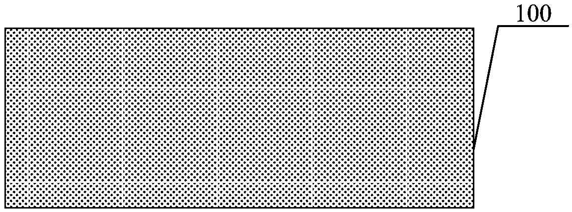
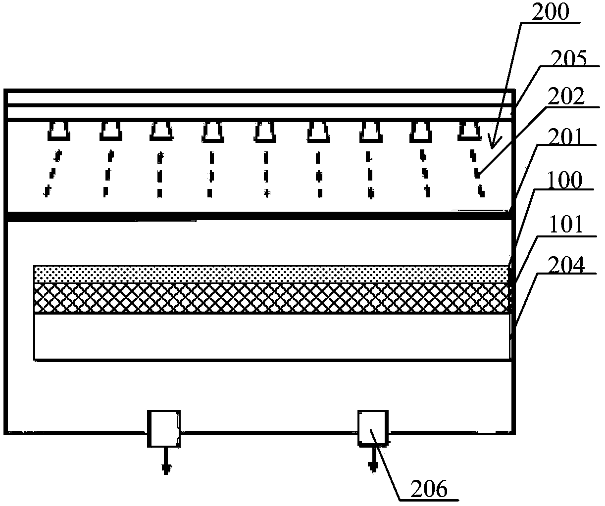
[0053] Such as Figure 1~5 Shown, the present invention provides a kind of post-hydrogenation treatment method of amorphous thin film, comprises steps:
[0054] An amorphous film 100 to be processed is provided, and the amorphous film 100 to be processed is placed in a reaction chamber 200 provided with a hot wire 201; a reaction gas is introduced into the reaction chamber 200, wherein the The hot wire 201 catalyzes and decomposes the reaction gas to generate at least hydrogen atoms, and radiates heat to the amorphous film 100 to be processed, so that the hydrogen atoms diffuse into the amorphous film 100 to be processed, so as to achieve Post-hydrogenation treatment of the amorphous film 100 to be treated.
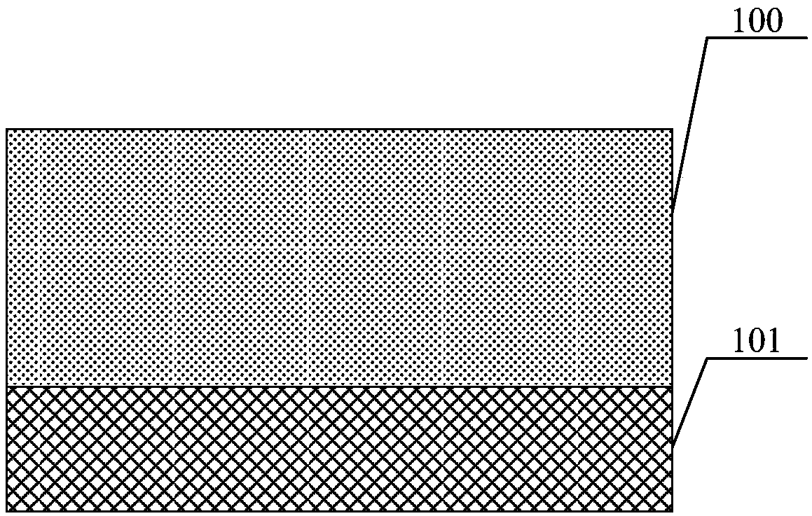
[0055] Such as Figure 1~2As shown, in the post-hydrogenation treatment method of the amorphous film of the present invention, firstly, an amorphous film 100 to be treated is provided;
[0056] As an example, the provided amorphous thin film 100 to be processed is form...
Embodiment 2
[0094] Such as Figure 6-7 As shown, the present invention also provides a method for preparing a silicon heterojunction solar cell structure, wherein the silicon heterojunction solar cell is preferably prepared based on the untreated amorphous film processed by the post-hydrogenation treatment method of the present invention, and the The method for preparing the silicon heterojunction solar cell structure includes the step of preparing a window layer, and the window layer is obtained through post-hydrogenation treatment as described in any one of the first embodiment.
[0095] Specifically, the present invention also provides a method for preparing a silicon heterojunction solar cell structure. In the solar cell heterostructure, the window layer includes intrinsic and n-type doped amorphous thin film materials, and the amorphous thin film material After the post-hydrogenation treatment in Embodiment 1, the treated window layer material has a higher optical band gap and a lowe...
PUM
| Property | Measurement | Unit |
|---|---|---|
| thickness | aaaaa | aaaaa |
| thickness | aaaaa | aaaaa |
| thickness | aaaaa | aaaaa |
Abstract
Description
Claims
Application Information


