Gallium nitride-based light emitting diode epitaxial wafer and manufacturing method thereof

A light-emitting diode, gallium nitride-based technology, applied in the direction of electrical components, circuits, semiconductor devices, etc., can solve the problems of weak carrier lateral expansion ability, low electron and hole recombination efficiency, etc., to improve recombination efficiency, improve The effect of luminous efficiency

Active Publication Date: 2019-03-15
HC SEMITEK SUZHOU
View PDF9 Cites 1 Cited by
  • Summary
  • Abstract
  • Description
  • Claims
  • Application Information

AI Technical Summary

Problems solved by technology

[0006] Embodiments of the present invention provide a gallium nitride-based light-emitting diode epitaxial wafer and a manufacturing method thereof, which can solve the problem of weak lateral expansion of carriers in semiconductor materials in the prior art, resulting in the gap between electrons and holes in the active layer. The problem of low compound efficiency

Method used


Image

  • Gallium nitride-based light emitting diode epitaxial wafer and manufacturing method thereof
  • Gallium nitride-based light emitting diode epitaxial wafer and manufacturing method thereof
  • Gallium nitride-based light emitting diode epitaxial wafer and manufacturing method thereof

Examples


Embodiment Construction

[0027] In order to make the object, technical solution and advantages of the present invention clearer, the implementation manner of the present invention will be further described in detail below in conjunction with the accompanying drawings.

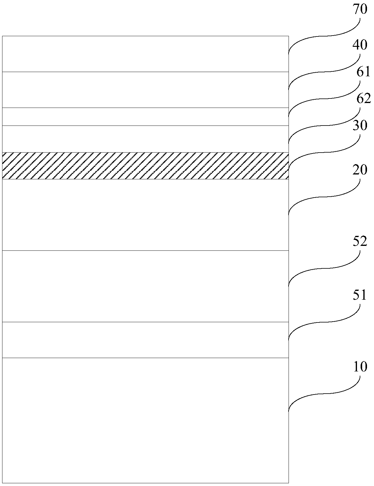
[0028] An embodiment of the present invention provides a GaN-based light-emitting diode epitaxial wafer. figure 1 A schematic structural diagram of a gallium nitride-based light-emitting diode epitaxial wafer provided by an embodiment of the present invention. see figure 1 , the GaN-based light-emitting diode epitaxial wafer includes a substrate 10, an N-type semiconductor layer 20, an active layer 30, and a P-type semiconductor layer 40, and the N-type semiconductor layer 20, the active layer 30, and the P-type semiconductor layer 40 are sequentially stacked on the substrate 10.

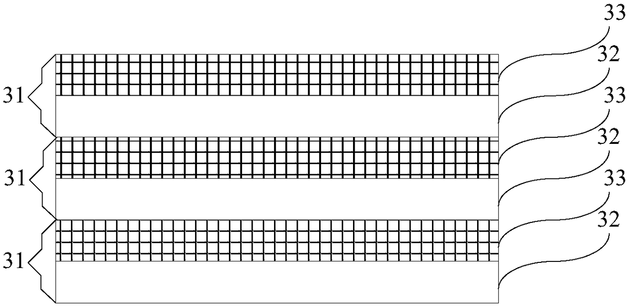
[0029] figure 2 A schematic structural diagram of an active layer provided by an embodiment of the present invention. see figure 2 , the active layer...


PUM


Abstract

The present invention discloses a gallium nitride-based light emitting diode epitaxial wafer and a manufacturing method thereof, and belongs to the technical field of semiconductors. The gallium nitride-based light emitting diode epitaxial wafer comprises a substrate, an N-type semiconductor layer, an active layer, and a P-type semiconductor layer, wherein the N-type semiconductor layer, the active layer, and the P-type semiconductor layer are sequentially stacked on the substrate. The active layer comprises a plurality of periodic structures stacked in sequence, and each of the periodic structures comprises a quantum well and a quantum barrier stacked in sequence; and a plurality of composite structures are inserted into the quantum barriers, and each of the composite structures comprisesa P-type doped gallium nitride layer, an undoped aluminum gallium nitride layer, and an N-type doped gallium nitride layer which are sequentially stacked. According to the technical scheme of the present invention, a plurality of composite structures are inserted into a quantum barrier layer, and each composite structure comprises a P-type doped gallium nitride layer, an undoped aluminum galliumnitride layer, and an N-type doped gallium nitride layer which are sequentially stacked, so that good two-dimensional electron gas can be formed, and the current expansion can be increased.

Description

technical field [0001] The invention relates to the technical field of semiconductors, in particular to a gallium nitride-based light-emitting diode epitaxial wafer and a manufacturing method thereof. Background technique [0002] A light-emitting diode (English: Light Emitting Diode, referred to as: LED) is a semiconductor electronic component that can emit light. LED has attracted widespread attention due to its advantages of energy saving, environmental protection, high reliability, and long service life. Since civil lighting focuses on energy saving and service life of products, it is particularly critical to reduce the series resistance of LEDs and improve the antistatic ability of LEDs. [0003] Epitaxial wafers are the primary products in the LED manufacturing process. The existing LED epitaxial wafer includes a substrate, an N-type semiconductor layer, an active layer and a P-type semiconductor layer, and the N-type semiconductor layer, the active layer and the P-t...

Claims


Application Information

Patent Timeline
Patent Type & Authority Applications(China)
IPC IPC(8): H01L33/14H01L33/20H01L33/32H01L33/00
CPCH01L33/0075H01L33/145H01L33/20H01L33/32H01L33/325
Inventor 葛永晖郭炳磊王群吕蒙普胡加辉李鹏
Owner HC SEMITEK SUZHOU
Why Eureka
Try Eureka