
Instrument and method for detecting LED chip

A technology of LED chips and detectors, which is applied in the direction of instrumentation, optical instrument testing, and electrical measurement, and can solve problems such as inaccurate testing, inability to accurately collect optical signals of the tested chip, and mutual influence

Active Publication Date: 2019-03-19
广州市鸿利秉一光电科技有限公司
View PDF10 Cites 2 Cited by
  • Summary
  • Abstract
  • Description
  • Claims
  • Application Information

AI Technical Summary

Problems solved by technology

[0003] The first detection method is to package the LED chip into an LED light source, and then connect a driving power supply at both ends of the LED light source, and then test the voltage at the test point of the LED light source to determine whether the electrical characteristics of the LED chip are within a reasonable range. However, this method requires the LED chip to be packaged into a finished product and then tested, and a driving power supply needs to be connected to both ends of the LED light source, so that if the driving power is not selected properly or is unstable, it will easily cause damage to the LED chip, resulting in inaccurate testing;
[0004] The second detection method, such as the US invention patent US006670820B2, discloses a method for detecting the electroluminescence characteristics of semiconductor materials and devices, specifically disclosing that excitation light is applied to the LED chip, and a forward direction is applied between the P region and the N region. The bias voltage forms a traction electric field to attract electrons in the P region and N region to move to the active region in the middle, and then radiative recombination occurs in the active region to emit light, and then the light receiving device is used to combine the intensity of the excitation light and the absorption of the chip coefficient, calculate the concentration of photogenerated carriers, combine the radiation luminescence of the active region and the concentration of carriers that are actually injected into the active region, and then quantitatively analyze the electronic luminescence performance of the measured LED chip. The detection method needs to remove the bias voltage applied to the chip, so it is easily affected by the bias voltage, which leads to the accuracy of the test part;
[0005] The third detection method, such as the Chinese patent application number CN200810070112.9, the announcement date is 2010.11.10, specifically discloses that by detecting the luminescence of the PN junction of the device under test under the irradiation of controllable excitation light, the luminescence characteristics and electric current of the LED chip can be improved. The characteristics are detected, wherein the electrical characteristic parameters include forward current and forward voltage, wherein the forward current is obtained by converting between the measured photoluminescence intensity and the photoluminescence intensity of the reference sample, and the forward bias voltage is obtained by The measured wavelength of the PN junction of the device under test is obtained through conversion, so the forward voltage must first obtain the optical characteristics of the PN junction of the test device, which mainly uses a light receiving device to obtain the optical characteristics of the LED chip and then determine the electrical characteristics, but due to the optical receiver It is located on one side of the chip under test to collect the optical signal of the chip under test, which makes it impossible to collect all the optical signals of the chip under test. In addition, the controllable excitation light is not completely isolated from the light emission of the chip under test, so that the controllable excitation light The light emitted by the chip under test will interact with each other, so that the optical signal of the chip under test cannot be accurately collected. In addition, if the entire LED chip needs to be tested, the light emitted by the entire LED chip will affect each other, resulting in the inability to accurately collect the light signal. Collect the optical signal of the chip under test; therefore, a test method with high test accuracy and no external power supply is required

Method used


Image

  • Instrument and method for detecting LED chip
  • Instrument and method for detecting LED chip
  • Instrument and method for detecting LED chip

Examples


Embodiment 1

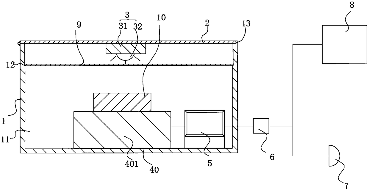
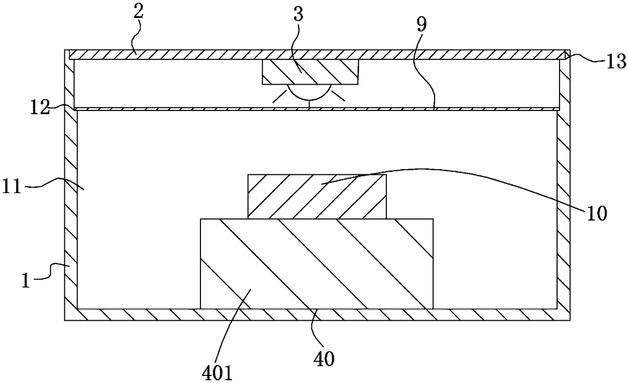
[0030] Such as figure 1 with figure 2 As shown, the instrument for testing LED chips includes a housing 1 , a cover plate 2 , an ultraviolet excitation light source 3 , a test area 40 for an LED chip to be tested, and an electrical characteristic detector 5 . In this embodiment, the electrical characteristic detector 5 is a voltage detector.

[0031] The casing 1 has a cavity 11 , an opening communicating with the cavity 11 is opened at the upper end of the casing 11 , and a step 12 is provided at the upper end of the inner wall of the casing 11 . The cover plate 2 is hinged at one end of the housing 1 and can cover the opening. The cover plate 2 is supported by the stepped surface 13 at the upper end of the housing except for one side of the hinge.

[0032] The ultraviolet excitation light source 3 is installed on the bottom surface of the cover plate 2, in order to better install and disassemble the ultraviolet excitation light source 3, as Figure 3 to Figure 6 As shown...

Embodiment 2

[0045] Such as figure 1 with figure 2 As shown, the instrument for testing LED chips includes a housing 1 , a cover plate 2 , an ultraviolet excitation light source 3 , a test area 40 for an LED chip to be tested, and an electrical characteristic detector 5 . In this embodiment, the electrical characteristic detector 5 is a current detector. Such as Figure 11 The volt-ampere characteristic curve of the LED chip shown shows that when the LED chip reaches the forward voltage VF, the current value of the LED chip is very small, and when the chip is excited by an ultraviolet excitation light source, the current generated inside the chip may not reach the normal value. With forward current, thereby in order to prevent that the electrical characteristic value cannot be detected, an amplifier (not shown in the figure) is also provided between the tested LED chip test area 40 and the electrical characteristic detector 5, and the amplifier is used to amplify the Measure the electr...

Embodiment 3

[0060] The difference between this embodiment and Implementation 1 is that the electrical characteristic detector 5 in the instrument for detecting LED chips is a voltage detector and a current detector, that is, the voltage detector and the current detector put

[0061] placed in the same housing to form an electrical characteristic detector.

[0062] The method for detecting LED chips using the above-mentioned instrument for detecting LED chips includes the following steps.

[0063] 1) Pre-store dead light curves and normal conduction curves corresponding to different LED chip ultraviolet excitation light sources and LED chip current values, and dead light curves and normal conduction curves corresponding to voltage values ​​in the controller. Generally speaking, for the same chip, the dead light curve and normal conduction curve are unique.

[0064] 2) The ultraviolet excitation light source 3 irradiates the LED chip 10 to be tested. The LED chip to be tested is a visible ...


PUM


Abstract

The invention discloses an instrument and method for detecting an LED chip. The instrument comprises an ultraviolet excitation light source, a test area of the tested LED chip and an electric characteristic detector. The test area of the tested LED chip is arranged opposite to the ultraviolet excitation light source and located in a radiation range of the ultraviolet excitation light source, and the electric characteristic detector is electrically connected to the test area of the tested LED chip. The method includes the steps that 1, the ultraviolet excitation light source irradiates the tested LED chip, wherein the wavelength of the tested LED chip is greater than that of the ultraviolet excitation light source; 2, an electric characteristic value of the tested LED chip is detected; 3, according to a corresponding relationship between the electric characteristic value of the tested LED chip and an irradiation illuminance value of the ultraviolet excitation light source, test conditions of the tested LED chip are determined. According to the instrument and method for detecting the LED chip, the detection of the LED chip can be realized without an external power supply, and meanwhile the abnormal conditions of the LED chip can be accurately detected.

Description

technical field [0001] The invention relates to the detection field of LED chips, in particular to an instrument and method for detecting LED chips. Background technique [0002] LED (light-emitting diode) is widely used in lighting, indication and other fields due to its long life, no pollution, and low energy consumption. In order to ensure the normal use of LED chips, it is generally necessary to test the electrical properties of LED chips. Existing The detection methods of LED chips include the following: [0003] The first detection method is to package the LED chip into an LED light source, and then connect a driving power supply at both ends of the LED light source, and then test the voltage at the test point of the LED light source to determine whether the electrical characteristics of the LED chip are within a reasonable range. However, this method requires the LED chip to be packaged into a finished product and then tested, and a driving power supply needs to be c...

Claims


Application Information

Patent Timeline
IPC IPC(8): G01R31/28G01M11/02
CPCG01M11/00G01R31/2851
Inventor 任荣斌汤乐明李东明何绍勇吴乾
Owner 广州市鸿利秉一光电科技有限公司
Features
  • Generate Ideas
  • Intellectual Property
  • Life Sciences
  • Materials
  • Tech Scout
  • Unparalleled Data Quality
  • Higher Quality Content
  • 60% Fewer Hallucinations
Learn More