Optical Microfluidic Chip Based on Polymer and Multilayer Metal Nanoparticle Modification

A microfluidic chip and nanoparticle technology, applied in scientific instruments, fluorescence/phosphorescence, laboratory containers, etc., can solve the problems of complicated and expensive instruments and equipment, need to drive pumps, and slow detection speed, etc. The effect of detection, elimination of interference, and improvement of detection sensitivity

Active Publication Date: 2020-06-26
INST OF ELECTRONICS CHINESE ACAD OF SCI
View PDF10 Cites 0 Cited by
  • Summary
  • Abstract
  • Description
  • Claims
  • Application Information

AI Technical Summary

Problems solved by technology

[0006] The present invention proposes an optical microfluidic chip based on polymer and multi-layer metal nanoparticle modification, which is used for fast, sensitive and convenient detection of low-concentration substances in micro-sample, and solves the complexity of existing detection methods. Expensive, not convenient, many detection steps, need to drive pumps and other devices, slow detection speed and other problems

Method used


Image

  • Optical Microfluidic Chip Based on Polymer and Multilayer Metal Nanoparticle Modification
  • Optical Microfluidic Chip Based on Polymer and Multilayer Metal Nanoparticle Modification
  • Optical Microfluidic Chip Based on Polymer and Multilayer Metal Nanoparticle Modification

Examples


Embodiment 1

[0061] Embodiment 1 (upper excitation mode)

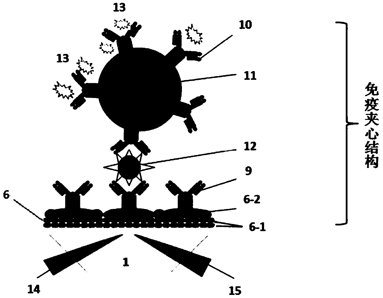
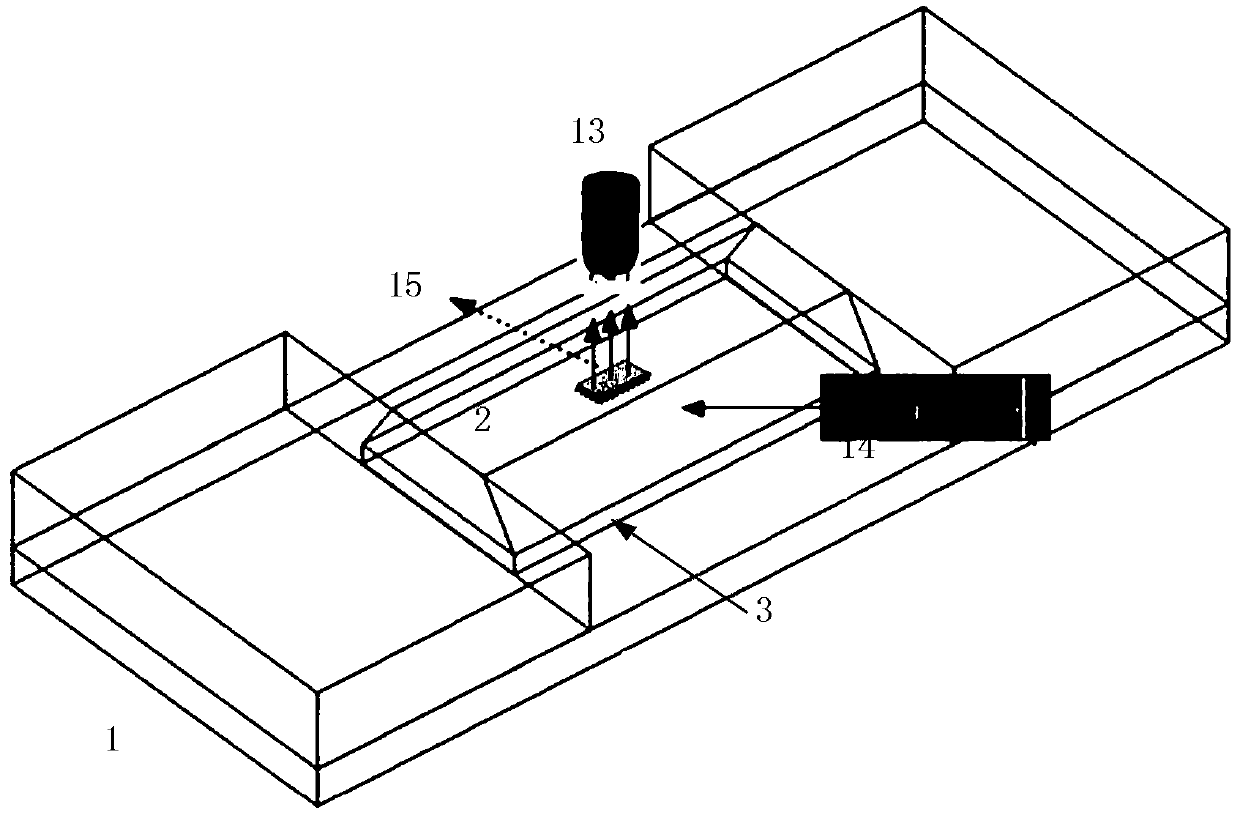
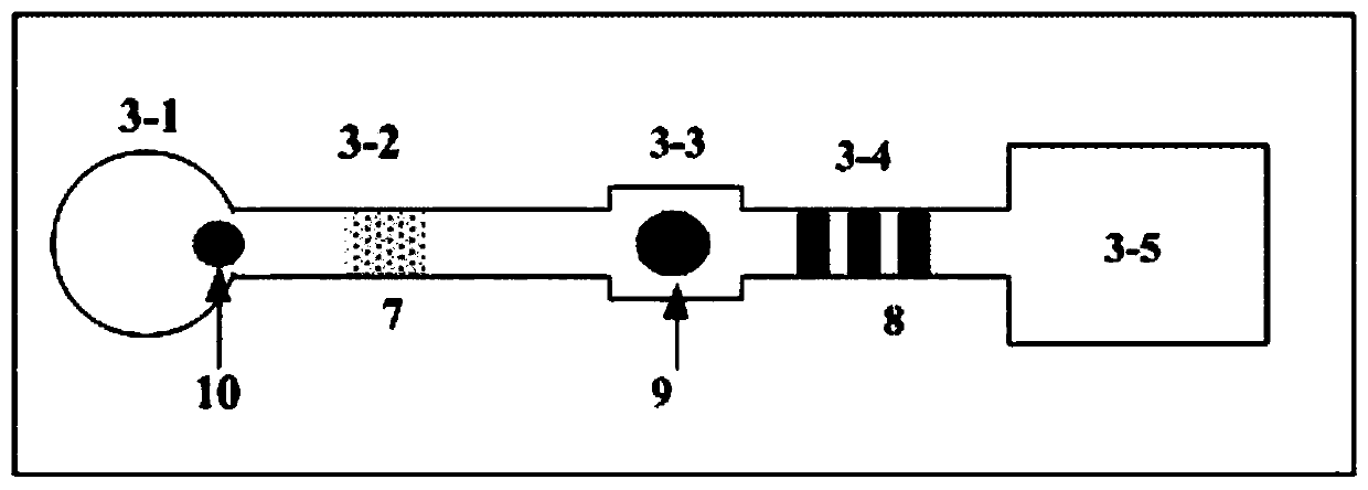
[0062] The chip bottom plate 1 and the chip channel layer 3 are prepared by one-step micro-injection molding. The thickness of the bottom plate is 0.5-10mm. It is preferably made of PET and PMMA high-transparency polymer materials, which have good optical transparency and stability, and the incident light is from the side below Optical surface collimation input. The micro-injection molding technology takes into account the flatness of the optical surface and the micron-level precision requirements of the channel, and realizes the micro-column / micro-disk array structure in the sampling channel area, which is conducive to the miscible reaction of reagents and the control of sampling time. The incident slope has mirror-level smoothness to achieve efficient coupling input and output of incident light. The incident angle of the groove is greater than 40 degrees. The incident light adopts 600nm monochromatic light, which can be polarized...

Embodiment 2

[0069] Embodiment 2 (lower excitation mode)

[0070] The chip bottom plate 1 and the chip channel layer 3 are prepared by one-step micro-injection molding. The thickness of the bottom plate is 0.5-10mm. It is preferably made of PET and PMMA high-transparency polymer materials, which have good optical transparency and stability, and the incident light is from the side below Optical surface collimation input. The micro-injection molding technology takes into account the flatness of the optical surface and the micron-level precision requirements of the channel, and realizes the micro-column / micro-disk array structure in the sampling channel area, which is conducive to the miscible reaction of reagents and the control of sampling time. The incident slope has mirror-level smoothness to achieve efficient coupling input and output of incident light. The incident angle of the groove is greater than 40 degrees. The incident light adopts 600nm monochromatic light, which can be polarized...


PUM

PropertyMeasurementUnit
thicknessaaaaaaaaaa
thicknessaaaaaaaaaa

Abstract

The invention provides an optical microfluidic chip. The optical microfluidic chip comprises a chip channel layer (3), wherein the chip channel layer comprises a sample injection zone (3-1), a sampleinjection channel (3-2), an optical detection zone (3-3), a waste liquid channel (3-4) and a waste liquid storage zone (3-5); a miscible microstructure (7) is arranged inside the sample injection channel (3-2); at least one section of time-controlled dissolving film (8) is arranged inside the waste liquid channel (3-4); a fluorescence detection component (13) is arranged on the optical detection zone (3-3); a capture antibody / identifier (9) is arranged inside the optical detection zone (3-3); a labeled antibody / identifier (10) is arranged at an inlet of the sample injection channel (3-2); a bottom chip plate (1) and an upper chip cover plate (2) are arranged on the two sides of the chip channel layer (3); the bottom chip plate (1) is modified by a polymer and multilayer metal nanoparticlemodification layer (6). The optical microfluidic chip is high in sensitivity during detection and is not interfered by incident light and superfluous fluorescent particles; in addition, a complex pumpvalve and other devices and equipment are not needed, so that rapid on-site detection is facilitated.

Description

technical field [0001] The invention relates to the technical field of biosensor detection, in particular to an optical microfluidic chip modified based on polymers and multilayer metal nanoparticles. Background technique [0002] Total internal reflection optical detection and total internal reflection fluorescence detection have the advantages of low background noise and are widely used in biomedical detection. Among them, total reflection fluorescence technology is a new type of optical detection technology, which uses the evanescent field generated by total reflection to excite fluorescence, so that the fluorescent particles within 200 nanometers of the incident light interface are excited to produce fluorescence, while the incident light and redundant other The fluorescent particles in the area will not interfere with the detection, and the color and turbidity of the sample will not affect the detection. Therefore, the detection signal-to-noise ratio is high. [0003] ...

Claims


Application Information

Patent Timeline
Patent Type & Authority Patents(China)
IPC IPC(8): G01N33/543G01N33/533G01N21/64B01L3/00
CPCB01L3/5027G01N21/64G01N33/533G01N33/543
Inventor 刘春秀薛宁孙建海徐成华蔡浩原李彤
Owner INST OF ELECTRONICS CHINESE ACAD OF SCI
Why Eureka
Try Eureka