

4H-SiC metal semiconductor field effect transistor with lightly doped gate edge drain side portion
A field-effect transistor and metal-semiconductor technology, applied in the field of 4H-SiC metal-semiconductor field-effect transistors, can solve the problems of easy breakdown of the device, limit the working environment and reliability of the device, and influence on its life, and reduce the carrier concentration. , The effect of alleviating the charging effect and improving the lifespan
- Summary
- Abstract
- Description
- Claims
- Application Information
AI Technical Summary
Problems solved by technology
Method used
Image

Examples
Embodiment 1
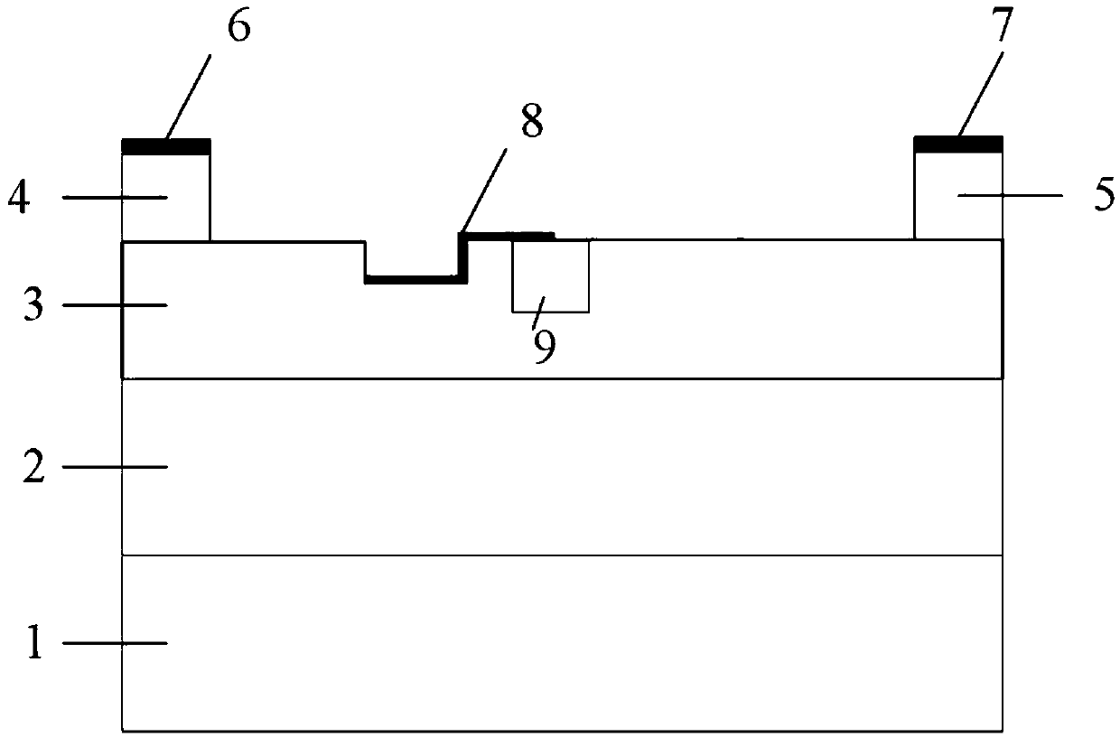
[0018] Such as figure 1 As shown, the 4H-SiC metal-semiconductor field-effect transistor with lightly doped gate edge and drain side parts provided in this embodiment includes a 4H-SiC semi-insulating substrate 1, a P-type buffer layer 2, and an N-type channel from bottom to top. Channel layer 3, the upper surface of the N-type channel layer 3 is provided with a source cap layer 4 and a drain cap layer 5, the upper surface of the source cap layer 4 is provided with a source electrode 6, and on the drain cap layer 5 A drain electrode 7 is provided on the surface, a gate electrode 8 is provided at the bottom of the N-type channel layer 3 and on the side close to the source cap layer 4, and a gate electrode 8 is provided at the bottom of the N-type channel layer 3 and is located under the gate of a part of the gate electrode 8 and part of the gate A lightly doped region 9 is formed between the drains, and the lightly doped region 9 has an axisymmetric structure taking the vertica...
PUM
| Property | Measurement | Unit |
|---|---|---|
| Depth | aaaaa | aaaaa |
| Length | aaaaa | aaaaa |
| Doping concentration | aaaaa | aaaaa |
Abstract
Description
Claims
Application Information