Trench type MOS field effect transistor and method, and electronic device

A field effect transistor, trench technology

Pending Publication Date: 2021-03-05
BYD SEMICON CO LTD
View PDF8 Cites 0 Cited by
  • Summary
  • Abstract
  • Description
  • Claims
  • Application Information

AI Technical Summary

Problems solved by technology

[0003] However, due to the design of the trench in the trench-gate SiC MOSFET device, there is an electric field concent...

Method used


Image

  • Trench type MOS field effect transistor and method, and electronic device
  • Trench type MOS field effect transistor and method, and electronic device
  • Trench type MOS field effect transistor and method, and electronic device

Examples


Embodiment Construction

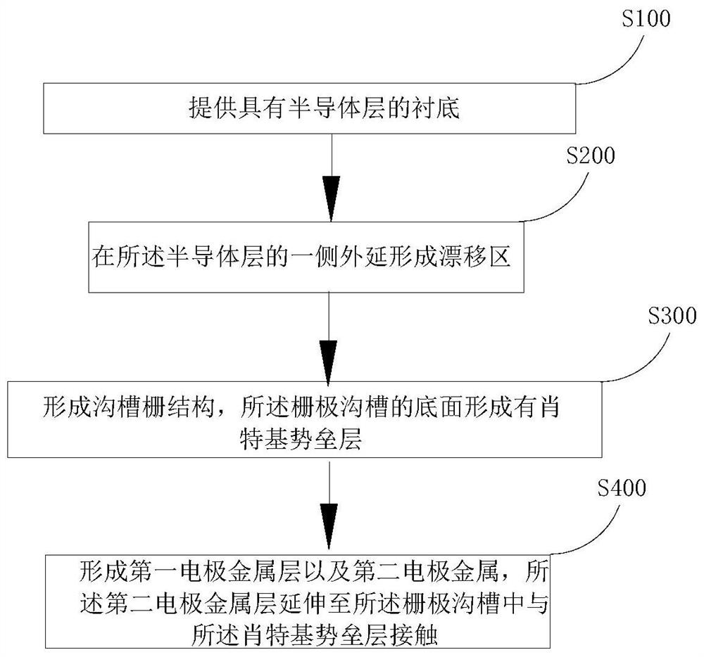
[0016] Embodiments of the present invention are described in detail below, examples of which are shown in the drawings, wherein the same or similar reference numerals designate the same or similar elements or elements having the same or similar functions throughout. The embodiments described below by referring to the figures are exemplary only for explaining the present invention and should not be construed as limiting the present invention.

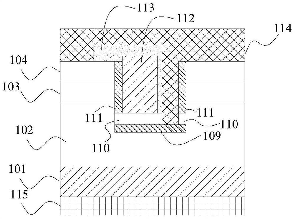
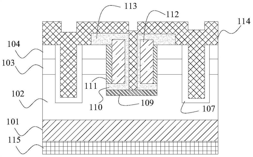
[0017] In one aspect of the present invention, the present invention provides a trench type MOS field effect transistor. According to an embodiment of the present invention, refer to figure 1 , the field effect transistor includes a first electrode metal layer 115 , a semiconductor layer 101 , and a drift region 102 . Those skilled in the art can understand that the trench MOS field effect transistor may also have a channel region 103 and a source region 104 on a side of the drift region 102 away from the semiconductor layer 101 . The ...


PUM

PropertyMeasurementUnit
Thicknessaaaaaaaaaa
Epitaxial thicknessaaaaaaaaaa

Abstract

The invention discloses a trench type MOS field effect transistor and a preparation method thereof, and an electronic device. The field effect transistor comprises a first electrode metal layer, a semiconductor layer and a drift region located on the side, away from the first electrode metal layer, of the semiconductor layer; a trench gate structure which is located on the side, away from the semiconductor layer, of the drift region and extends into the drift region, wherein the trench gate structure comprises a gate located in a gate trench, a Schottky barrier layer is arranged on the bottomsurface of the gate trench, and a gate isolation medium is arranged between the Schottky barrier layer and the gate; and a second electrode metal layer which extends into the gate trench and is in contact with the Schottky barrier layer, wherein an electrical isolation medium is arranged between the second electrode metal layer and the gate. The trench type MOS field effect transistor can utilizethe SBD device to isolate the influence of a high electric field on the gate medium at the bottom of the trench, especially at the corner during reverse voltage withstanding.

Description

technical field [0001] The invention relates to the field of electronics, in particular to a trench type MOS field effect transistor, a method, and an electronic device. Background technique [0002] Due to the advantages of high thermal conductivity, high breakdown field strength, and high electron saturation velocity, SiC material is suitable for making semiconductor devices with high power, high voltage, high operating temperature, and high operating frequency power. MOSFET (Metal-Oxide Semiconductor Field-Effect Transistor) power devices based on SiC materials have the advantages of low power consumption, high withstand voltage, high frequency, good heat dissipation, and miniaturization. It is widely used in high voltage and high current places. The trench gate SiC MOSFET has a smaller specific on-resistance than the planar SiC MOSFET, so it has better application prospects. [0003] However, due to the design of the trench in the trench-gate SiC MOSFET device, there i...

Claims


Application Information

Patent Timeline
IPC IPC(8): H01L29/78H01L29/423H01L21/336
CPCH01L29/66613H01L29/78H01L29/4236
Inventor 刘东庆
Owner BYD SEMICON CO LTD
Why Eureka
Try Eureka