HEMT device based on double heterojunctions and composite passivation layer, and preparation method thereof

A technology of double heterojunction and passivation layer, applied in semiconductor/solid-state device manufacturing, semiconductor devices, electrical components, etc., can solve the problems affecting high electron mobility transistors, insufficient electron transfer rate, serious self-heating effect, etc. The effect of improving high temperature reliability, suppressing self-heating effect, and improving internal electric field distribution

Pending Publication Date: 2021-12-21
瑶芯微电子科技(上海)有限公司
View PDF0 Cites 0 Cited by
  • Summary
  • Abstract
  • Description
  • Claims
  • Application Information

AI Technical Summary

Problems solved by technology

[0003] However, when applied to high power or high frequency, β-Ga 2 o 3 The substrate has problems such as insufficient electron transmission rate and low thermal conductivity, which lead to serious self-heating effect, which greatly affects the performance of High Electron Mobility Transistor (HEMT) devices.

Method used


Image

  • HEMT device based on double heterojunctions and composite passivation layer, and preparation method thereof
  • HEMT device based on double heterojunctions and composite passivation layer, and preparation method thereof
  • HEMT device based on double heterojunctions and composite passivation layer, and preparation method thereof

Examples


Embodiment Construction

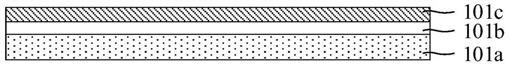
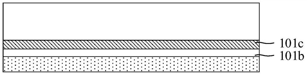
[0046] In order to improve the high-temperature reliability of the device, an embodiment of the present invention provides a HEMT device based on a double heterojunction and a composite passivation layer and a manufacturing method thereof. The scheme provided in this embodiment will be described in detail below with reference to the accompanying drawings.

[0047] In order to make the purpose, technical solutions and advantages of the embodiments of the present invention clearer, the embodiments of the present invention will be described in detail below with reference to the accompanying drawings. However, those skilled in the art can understand that in each embodiment of the present invention, many technical details are provided for readers to better understand the present application. However, even without these technical details and various changes and modifications based on the following embodiments, the technical solutions claimed in this application can also be realized. ...


PUM

PropertyMeasurementUnit
thicknessaaaaaaaaaa
thicknessaaaaaaaaaa
thicknessaaaaaaaaaa

Abstract

The invention discloses an HEMT device based on double heterojunctions and a composite passivation layer, and a preparation method thereof. The method comprises the following steps: carrying out the ion implantation of the upper surface of a first substrate to form a second substrate; forming a bonding intermediate layer on the upper surface of the second substrate, and transferring beta-Ga2O3 to the upper surface of the bonding intermediate layer to form a heterojunction substrate; growing a layer of beta-Ga2O3 on the upper surface of the heterojunction substrate as a buffer layer; sequentially growing a secondary barrier layer, a first doping layer, a first heterojunction layer, a quantum well layer, a second heterojunction layer, a second doping layer and a main barrier layer on the upper surface of the buffer layer; performing ion implantation on two sides of the upper surface of the main barrier layer to form a source ohmic contact region and a drain ohmic contact region; forming a source electrode on the source electrode ohmic contact region, and forming a drain electrode on the drain electrode ohmic contact region; sequentially growing an oxide layer and a dielectric layer on the upper surface of the main barrier layer; forming a grid electrode on the dielectric layer; and growing a passivation layer on the upper surface of the dielectric layer, and etching two sides of the dielectric layer and the passivation layer.

Description

technical field [0001] The invention belongs to the technical field of semiconductors, and in particular relates to a HEMT device based on a double heterojunction and a composite passivation layer and a preparation method thereof. Background technique [0002] β-Ga 2 o 3 As a new generation of semiconductor materials, due to β-Ga 2 o 3 The ultra-bandgap width and theoretical breakdown electric field strength of β-GaN are higher than those of SiC and GaN, and they are superior to SiC and GaN in terms of high temperature resistance, high pressure resistance and radiation resistance. Therefore, β-Ga 2 o 3 It is considered suitable for the preparation of next-generation power devices, such as diodes and field-effect transistors. [0003] However, when applied to high power or high frequency, β-Ga 2 o 3 The substrate has problems such as insufficient electron transmission rate and low thermal conductivity, which lead to serious self-heating effect, which greatly affects th...

Claims


Application Information

Patent Timeline
Patent Type & Authority Applications(China)
IPC IPC(8): H01L29/778H01L21/34
CPCH01L29/7782H01L21/34H01L29/66969
Inventor 李鑫
Owner 瑶芯微电子科技(上海)有限公司
Why Eureka
Try Eureka