
A submicron flow channel microfluidic chip and its manufacturing method

A microfluidic chip and sub-micron technology, which is applied in the fields of life science and medicine, can solve problems such as the inability to determine the volume of nanopore liquid and the inability to accurately detect the concentration of the sample to be tested.

Active Publication Date: 2021-07-30
TIANJIN UNIV
View PDF5 Cites 0 Cited by
  • Summary
  • Abstract
  • Description
  • Claims
  • Application Information

AI Technical Summary

Problems solved by technology

However, the traditional Coulter counter can only detect particles with a size similar to that of cells, while the nanopore detection method uses electrophoretic force to drive DNA and other molecules through the nanopore, so the volume of liquid passing through the nanopore cannot be determined, so the sample to be tested cannot be accurately detected concentration

Method used


Image

  • A submicron flow channel microfluidic chip and its manufacturing method
  • A submicron flow channel microfluidic chip and its manufacturing method
  • A submicron flow channel microfluidic chip and its manufacturing method

Examples


Embodiment 1

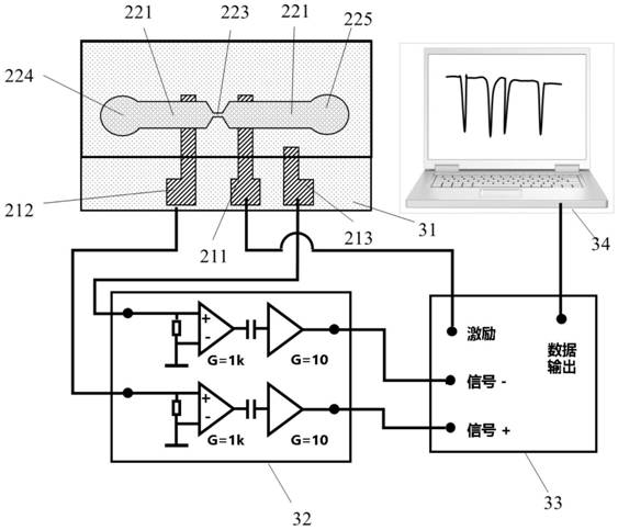
[0079] like figure 2 In (I), the application provides a submicron channel microfluidic chip, comprising:

[0080] A base layer 21, the upper surface of which is provided with an excitation electrode and a first detection electrode;

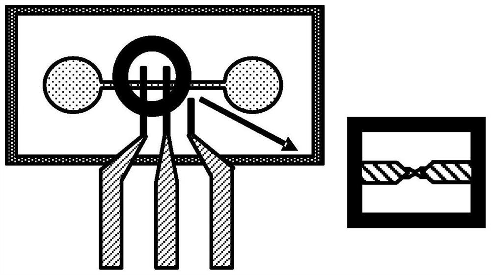
[0081] The upper substrate 22 is provided with a micro-nano channel 221 on its lower surface, and the channel width in the middle of the micro-nano channel 221 is less than 1 micron and is provided with protrusions 222; the lower surface of the upper substrate 22 and the base layer 21 Bonding on the upper surface of the upper surface, wherein the gap between the raised structure and the base layer forms a submicron flow channel 223;

[0082] Wherein, the excitation electrode 211 and the first detection electrode 212 are respectively located at both ends of the submicron channel 223 and arranged in contact with the micronano channel 221;

[0083] Wherein, the upper substrate is also provided with a reagent injection port 224 and an outlet 225 co...

Embodiment 2

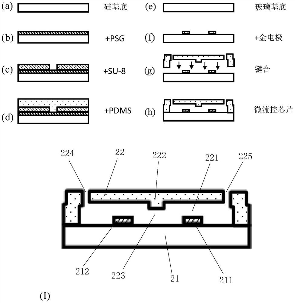
[0102] like Figure 5 As shown, based on the submicron flow channel microfluidic chip in Example 1, this embodiment also provides a method for manufacturing a submicron flow channel microfluidic chip, including steps:

[0103] S501, making an upper substrate with micro-nano channels on the lower surface; wherein, the flow channel in the middle of the micro-nano channels has a width less than 1 micron and is provided with protrusions; specifically, including:

[0104] S501.1, making a submicron flow channel template, including:

[0105] S501.1.1. Use piranha and hydrofluoric acid solution to clean the upper surface and polish a low-resistance silicon wafer to remove contamination and impurities on the surface of the silicon wafer; wherein, the piranha is a mixed solution of concentrated sulfuric acid and hydrogen peroxide , wherein the concentrated sulfuric acid: the volume ratio of hydrogen peroxide is 3:1; wherein, the low-resistance silicon chip is placed on the bottom of t...


PUM

PropertyMeasurementUnit
sizeaaaaaaaaaa
thicknessaaaaaaaaaa
thicknessaaaaaaaaaa

Abstract

The invention discloses a submicron channel microfluidic chip and a manufacturing method thereof, comprising: a base layer, the upper surface of which is provided with excitation electrodes and first detection electrodes; The middle section of the micro-nano channel has a channel width less than 1 micron and is provided with protrusions; the lower surface of the upper substrate is bonded to the upper surface of the base layer, wherein a structure formed between the structure provided with protrusions and the base layer A submicron flow channel; wherein, the excitation electrode and the first detection electrode are respectively located at both ends of the submicron flow channel and are arranged in contact with the micronano channel; wherein, the upper substrate is also provided with a The reagent injection port and the outlet communicated with the micro flow channel. From the above, the above-mentioned microfluidic chip of the present application has a detection sensitivity close to that of nanopores, and can be used for the detection and quantification of biological macromolecules such as plasmids and cellular exosomes.

Description

technical field [0001] The invention relates to the fields of life science and medicine, and particularly relates to a microfluidic chip with a submicron channel and a manufacturing method thereof. Background technique [0002] The detection and quantification of biological macromolecules such as plasmids and proteins are widely used in the fields of medicine, genetics, genetic engineering and biometric research. Especially in the field of biometric research, the establishment of a biological substance traceability system with clear traceability and the development of related measurement standards, so that the detection results of biological substances can be traced to SI units, is one of the most active fields in international measurement research. The main purpose of this project is to establish an accurate quantitative method for biological macromolecules based on single-molecule counting technology, establish a counting method directly traceable to SI units, realize the ...

Claims


Application Information

Patent Timeline
Patent Type & Authority Patents(China)
IPC IPC(8): B01L3/00
CPCB01L3/5027B01L3/502707B01L2200/10B01L2300/0645B01L2300/0861B01L2300/0887B01L2300/12
Inventor 段学欣刘建涛韩子钰陈雪娇刘展宁
Owner TIANJIN UNIV
Learn More