Method for processing solar cell piece

A solar cell sheet and processing method technology, which is applied in the field of solar cells, can solve the problems of complicated process and impracticality, and achieve the effect of simple process

Active Publication Date: 2019-04-09
JA SOLAR TECH YANGZHOU
View PDF5 Cites 2 Cited by
  • Summary
  • Abstract
  • Description
  • Claims
  • Application Information

AI Technical Summary

Problems solved by technology

This patent not only requires a mask layer, but also needs to enter the furnace tube for oxidation, the process is complicated and not practical

Method used


Image

  • Method for processing solar cell piece
  • Method for processing solar cell piece
  • Method for processing solar cell piece

Examples


Embodiment 1

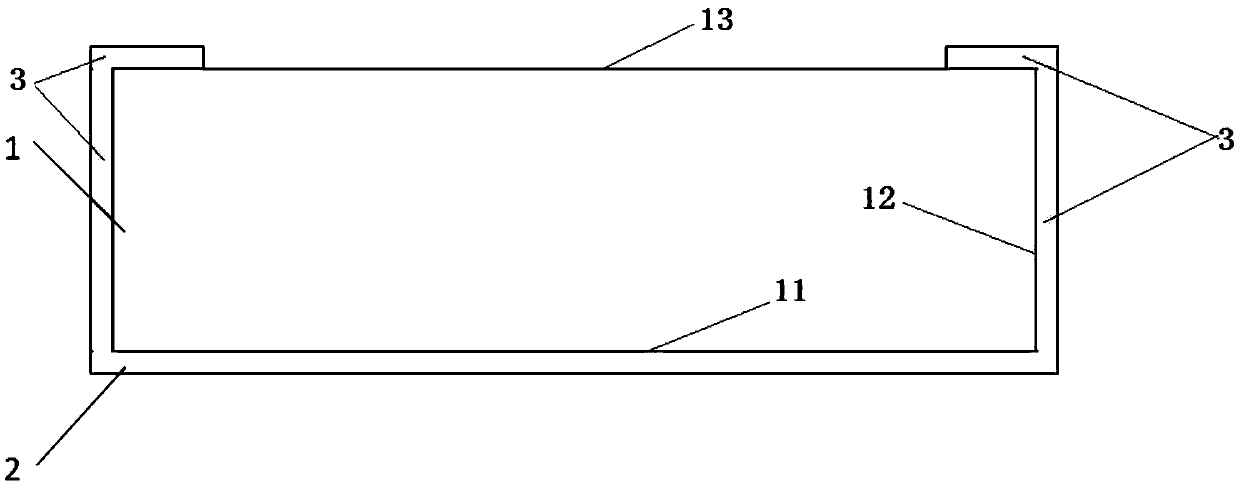
[0078] Using the solar cell processing method provided in this embodiment, that is, the solar cell structure after the silicon thin film asymmetric etching process is as follows Figure 6 As shown, a silicon substrate 1 is included, and a first silicon thin film layer 2 is provided on the first main surface of the silicon substrate 1 .

[0079] The thickness of the first silicon thin film layer is 100 nm.

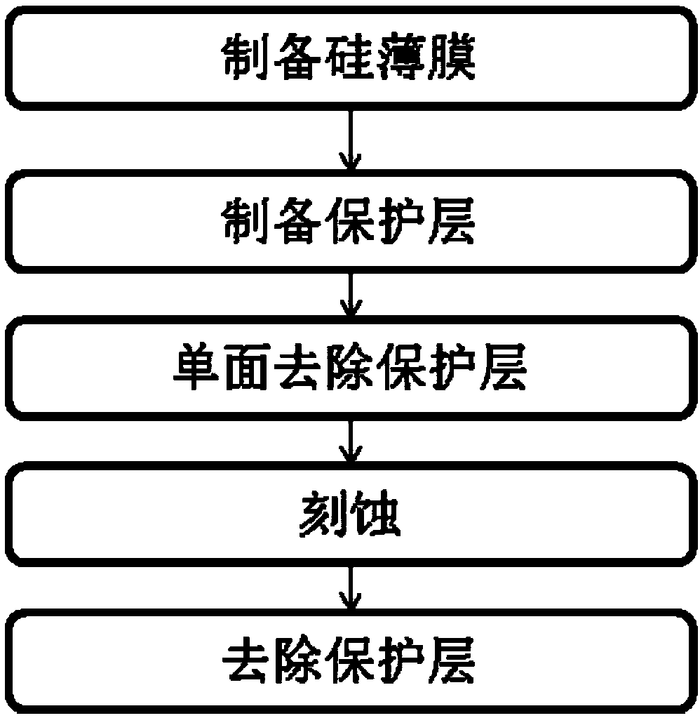
[0080] This embodiment illustrates a method for processing solar cells, which can also be called asymmetric etching of silicon thin films. This method is to remove the silicon thin film layer around the plating surface by pure chemical etching, such as figure 1 , including the following steps:

[0081] S1. Preparation of silicon thin film: place a clean silicon substrate 1 in a low-pressure chemical deposition (LPCVD) device to grow a 100nm non-doped first silicon thin film layer 2 and a second silicon thin film layer 3, wherein the first silicon thin film layer 2 is set ...

Embodiment 2

[0087] Using the solar cell processing method provided in this embodiment, that is, the solar cell structure after the silicon thin film asymmetric etching process is as follows Figure 6 As shown, a silicon substrate 1 is included, and a first silicon thin film layer 2 is provided on the first main surface of the silicon substrate 1 .

[0088] The thickness of the first silicon thin film layer is 200nm, including 100nm of undoped silicon thin film and 100nm of phosphorus (P) doped silicon thin film.

[0089] This embodiment illustrates a method for processing solar cells, which can also be called asymmetric etching of silicon thin films. This method is to remove the silicon thin film layer around the plating surface by pure chemical etching, such as figure 1 , including the following steps:

[0090] S1. Preparation of silicon thin film: place a clean silicon substrate 1 in a plasma chemical deposition (PECVD) device to grow a 100nm non-doped first silicon thin film layer 2 a...

Embodiment 3

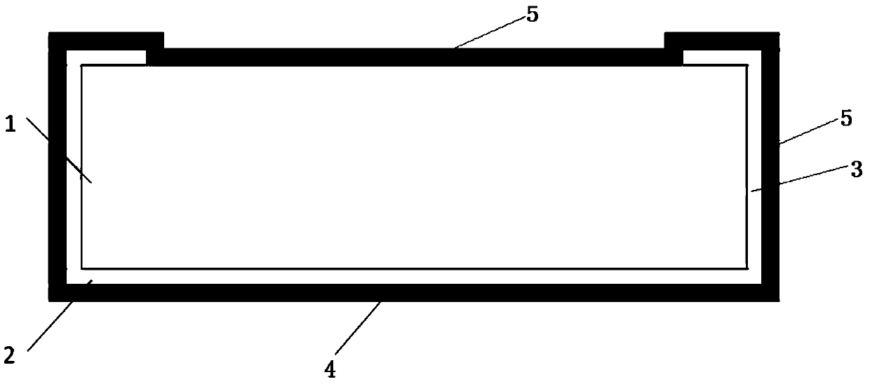
[0096] Using the solar cell processing method provided in this embodiment, that is, the solar cell structure after the silicon thin film asymmetric etching process is as follows Figure 7 As shown, a silicon substrate 1 is included, a passivation dielectric layer 6 (specifically a silicon oxide layer) is provided on the first main surface 11 of the silicon substrate 1 , and a first silicon thin film layer 2 is provided on the passivation dielectric layer 6 .

[0097] Wherein the passivation medium layer 6 has a thickness of 1.2 nm.

[0098] The thickness of the first silicon thin film layer 2 is 300nm, including 200nm undoped silicon thin film layer and 100nm phosphorus (P) doped silicon thin film layer.

[0099] This embodiment illustrates a method for processing solar cells, which can also be called asymmetric etching of silicon thin films. This method is to remove the silicon thin film layer around the plating surface by pure chemical etching, such as figure 1 , including ...


PUM

PropertyMeasurementUnit
thicknessaaaaaaaaaa
thicknessaaaaaaaaaa
thicknessaaaaaaaaaa

Abstract

The invention discloses a method for processing a solar cell piece, comprising the following steps: S1, providing a solar cell piece, wherein the solar cell piece comprises a silicon substrate, a first silicon thin film layer formed on a first main surface of the silicon substrate, and a second silicon thin film layer formed on partial surface of a second main surface of the silicon substrate andthe side surface of the silicon substrate; S2, using a chemical oxidation process to form a first protection layer on the first silicon thin film layer and to form a second protection layer on the surface of the second silicon thin film layer and on the surface, not forming the second silicon thin film layer, of the second main surface; S3, using a first etching solution to remove the second protection layer; S4, using a second etching solution to remove the second silicon thin film layer; and S5, using the first etching solution to remove the first protection layer so as to form a solar cellpiece with a silicon thin film on a single face. According to the method, a pure chemical method is adopted to realize single-side etching of the silicon thin film of a winding surface, and the process is simple and is not limited by the thickness of the silicon thin film.

Description

technical field [0001] The invention belongs to the technical field of solar cells, and in particular relates to a method for processing solar cells. Background technique [0002] In order to obtain high efficiency of crystalline silicon solar cells, the surface of the crystalline silicon substrate must have good passivation to control the surface recombination rate of minority carriers to a minimum, so as to obtain higher opening voltage, current and fill factor. The common method of silicon surface passivation is mainly to use silicon oxide, silicon nitride, silicon oxynitride, aluminum oxide, silicon and other single-layer or multi-layer dielectric film structures to inhibit the surface recombination rate by reducing the concentration of dangling bonds on the surface of the silicon substrate. [0003] In recent years, by growing an ultra-thin passivation dielectric layer (usually an oxide layer) and a doped silicon film on the back of the silicon substrate, and using the ...

Claims


Application Information

Patent Timeline
Patent Type & Authority Applications(China)
IPC IPC(8): H01L31/18
CPCH01L31/1804H01L31/186Y02E10/547Y02P70/50
Inventor 张俊兵王传红秦怡
Owner JA SOLAR TECH YANGZHOU
Why Eureka
Try Eureka