Resistance random access memory based on multiferroic heterostructure

A resistive memory and heterostructure technology, applied in the field of storage, can solve problems such as damage and difficulty in miniaturization, and achieve the effects of fast writing speed, favorable miniaturization, and good retention characteristics

Active Publication Date: 2019-04-09
UNIV OF SCI & TECH OF CHINA
View PDF8 Cites 6 Cited by
  • Summary
  • Abstract
  • Description
  • Claims
  • Application Information

AI Technical Summary

Problems solved by technology

However, ferroelectric random access memory based on ferroelectricity still uses charge as a storage medium, which is difficult to miniaturize for destructive reading

Method used


Image

  • Resistance random access memory based on multiferroic heterostructure
  • Resistance random access memory based on multiferroic heterostructure
  • Resistance random access memory based on multiferroic heterostructure

Examples


Embodiment Construction

[0029] The following will clearly and completely describe the technical solutions in the embodiments of the present invention with reference to the accompanying drawings in the embodiments of the present invention. Obviously, the described embodiments are only some, not all, embodiments of the present invention. Based on the embodiments of the present invention, all other embodiments obtained by persons of ordinary skill in the art without making creative efforts belong to the protection scope of the present invention.

[0030] In order to make the above objects, features and advantages of the present invention more comprehensible, the present invention will be further described in detail below in conjunction with the accompanying drawings and specific embodiments.

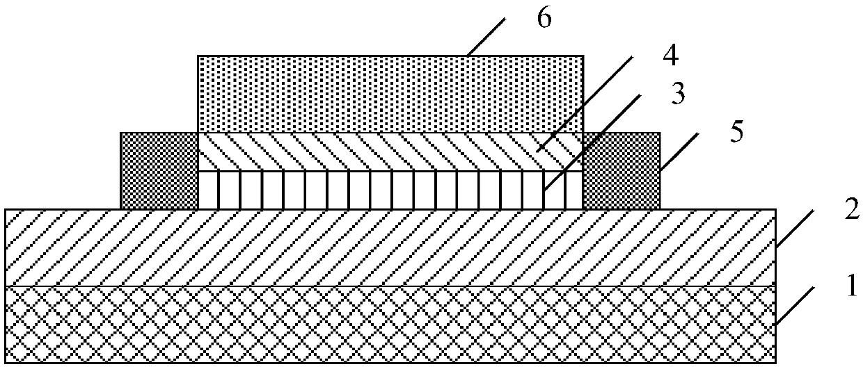
[0031] refer to figure 1 , figure 1 A schematic structural diagram of a resistive memory provided by an embodiment of the present invention, the resistive memory includes:

[0032] substrate1;

[0033] a ferrom...


PUM

PropertyMeasurementUnit
thicknessaaaaaaaaaa
thicknessaaaaaaaaaa
thicknessaaaaaaaaaa

Abstract

The invention provides a resistance random access memory based on multiferroic heterostructure. The resistance random access memory comprises a substrate, a ferromagnetic bottom electrode layer, a ferroelectric barrier layer, a ferromagnetic top electrode layer, an insulating layer, and a contact electrode lead layer, wherein the ferromagnetic bottom electrode layer is arranged on the substrate; the ferroelectric barrier layer is arranged at one side, deviated from the substrate, of the ferromagnetic bottom electrode layer, and the ferroelectric barrier layer partially covers the ferromagneticbottom electrode layer; the ferromagnetic top electrode layer is arranged at one side, deviated from the ferromagnetic bottom electrode layer, of the ferroelectric barrier layer, and the area of theferromagnetic top electrode layer is same as that of the ferroelectric barrier layer; the insulating layer is arranged on the ferromagnetic bottom electrode layer and surrounds the sidewall of the ferroelectric barrier layer and the sidewall of the ferromagnetic top electrode layer; and the contact electrode lead layer is arranged at one side, deviated from the ferroelectric barrier layer, of theferromagnetic top electrode layer. The memory has the features of being fast in writing speed and low in written current density and has multiple non-volatile memory states.

Description

technical field [0001] The invention relates to the technical field of storage, and more specifically, relates to a resistive variable memory based on a multiferroic heterostructure. Background technique [0002] Modern memory is developing towards high density, fast speed, low energy consumption, and safety and reliability. However, the pursuit of high-density characteristics requires the continuous reduction of the size of transistors. When reduced to nanometers, many quantum effects will appear, such as quantum tunneling. At this time, traditional silicon-based semiconductor devices will reach the physical and technological limits, so people need to develop new multifunctional materials and information storage and processing technologies. [0003] Flash memory and hard disk are non-volatile storage devices currently used, and the writing speed is relatively slow, on the order of 10 microseconds or even milliseconds. As the next generation of new memory devices, both phas...

Claims


Application Information

Patent Timeline
Patent Type & Authority Applications(China)
IPC IPC(8): H01L43/08H01L43/02
CPCH10N50/80H10N50/10
Inventor 黄伟川罗振殷月伟李晓光
Owner UNIV OF SCI & TECH OF CHINA
Why Eureka
Try Eureka