Method for preparing metal nanostructures by self-absorbing nanoimprinting

A metal nanostructure and nanoimprint technology, applied in nanotechnology, metal material coating process, vacuum evaporation plating, etc., can solve the problem of inability to complete the evaporation gold stripping process, rough etching of gold sidewalls, and increase template loss, etc. problem, to achieve the effect of low cost, low cost and easy application

Active Publication Date: 2020-01-21
INST OF SEMICONDUCTORS - CHINESE ACAD OF SCI
View PDF3 Cites 0 Cited by
  • Summary
  • Abstract
  • Description
  • Claims
  • Application Information

AI Technical Summary

Problems solved by technology

The high-temperature heating and cooling process will prolong the imprinting cycle and reduce the output rate, while high-pressure molding will increase template loss and limit the application of substrate materials that cannot withstand high pressure. Professional imprinting equipment is required to provide large-area uniform pressure and high temperature, expensive
In UV-cured nanoimprinting, the polymer is no longer heated and cooled to shape, but is cured by ultraviolet radiation. In order to make the template and the substrate fully bonded, it is necessary to apply a pressure above atmospheric pressure, which also requires expensive imprinting equipment. Auxiliary to prepare uniform
In actual imprinting, the structure of the imprinting glue is usually a positive mesa structure, which cannot complete the steam gold stripping process. Usually, nanoimprinting on the gold film and etching gold are used to complete the preparation of the gold nanostructure. This method costs High, and the etched gold sidewall is rough

Method used


Image

  • Method for preparing metal nanostructures by self-absorbing nanoimprinting
  • Method for preparing metal nanostructures by self-absorbing nanoimprinting
  • Method for preparing metal nanostructures by self-absorbing nanoimprinting

Examples


Embodiment Construction

[0035] In order to make the objectives, technical solutions and advantages of the present disclosure clearer, the present disclosure will be further described in detail below in conjunction with specific embodiments and with reference to the accompanying drawings.

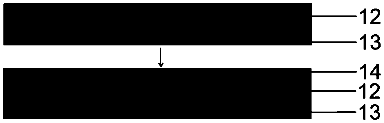
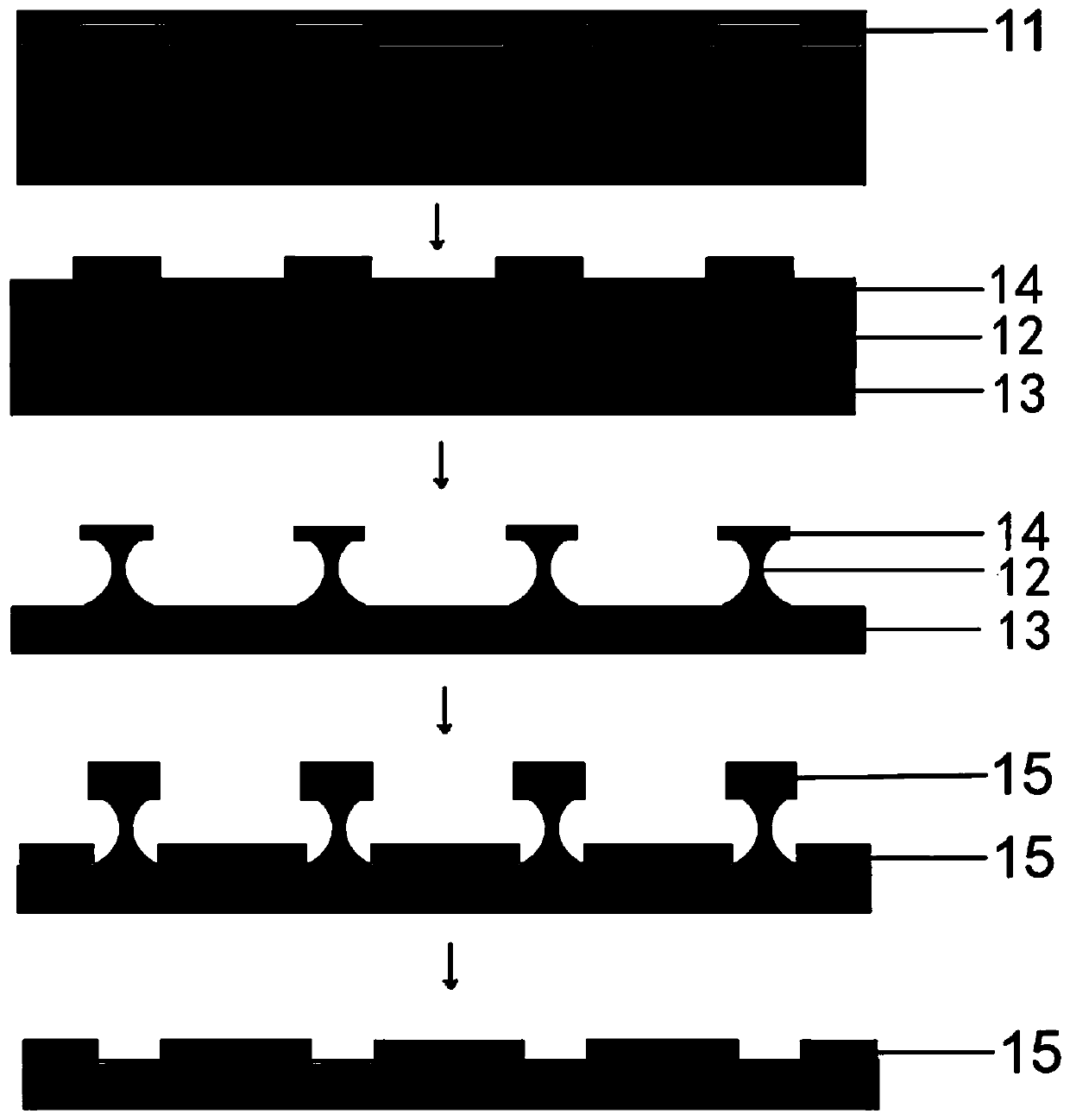
[0036] The present disclosure provides a large-area, low-cost self-absorption nanoimprinting method for preparing metal nanostructures, such as Figure 1-3 As shown, the method for preparing metal nanostructures by self-absorption nanoimprinting includes:

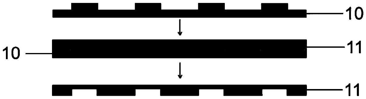
[0037] Step 1. Preparation of soft imprint template, such as figure 1 Shown:

[0038] Use the hard matrix nanoimprint template 10 to turn the mold to obtain the PDMS soft imprint template 11 (referred to as PDMS soft template), such as figure 1 As shown, the hard matrix nanoimprint template has nanostructures. Correspondingly, the PDMS soft imprint template obtained by remoulding also has nanostructures, and the two structures are opposite; using PDMS to remould the ha...


PUM


Abstract

The present disclosure provides a method for preparing a metal nanostructure through self-priming nanoimprinting. The method comprises the steps that polydimethylsiloxane (PDMS) is used for rollover on the surface of a hard-matrix nanoimprinting template, and a PDMS soft template is obtained; the surface of a substrate is spin-coated with a lower layer of glue, heating and curing are carried out,and the surface of the lower layer of glue is spin-coated with an upper layer of glue; the PDMS soft template is overlaid on the surface of the upper layer of glue, the upper layer of glue is heated and cured, the PDMS soft template is removed, and a grating structure is obtained; if being negative glue, the upper layer of glue is baked after being exposed, and if being positive glue, the upper layer of glue is not exposed; the upper layer of glue and the lower layer of glue on the substrate form a downfall structure by development; and metal is evaporated, the lower layer of glue, the upper layer of glue and metal located on the upper layer of glue are stripped through a stripping process, and the metal nanostructure is formed.

Description

Technical field [0001] The present disclosure relates to the technical field of micro-nano manufacturing, in particular to a method for preparing metal nano-structures by self-absorption nano-imprinting. Background technique [0002] With the development of nanoscience, its application extends to various fields, especially the preparation of nanostructures has gradually become a research hotspot. As early as 1995, Professor Zhou Yu, a Chinese scientist at Princeton University, proposed nanoimprint technology for the limitation of the exposure wavelength of the lithography process. The nano pattern on the template was imprinted on the substrate. The nanoimprint technology saved the lithography process. It can break the diffraction limit and prepare nanostructures in a large area. This technology has aroused the interest of many researchers, has been widely studied and applied, and has become a new generation of nanomanufacturing technology, which is applied in various fields of th...

Claims


Application Information

Patent Timeline
Patent Type & Authority Patents(China)
IPC IPC(8): C23C14/16C23C14/18C23C14/30C23C14/04B82Y40/00
CPCB82Y40/00C23C14/042C23C14/16C23C14/18C23C14/30
Inventor 耿照新苏玥吕晓庆裴为华陈弘达
Owner INST OF SEMICONDUCTORS - CHINESE ACAD OF SCI
Why Eureka
Try Eureka