A graphene-based high-emissivity infrared emission film and preparation method thereof
A technology with infrared emission and high emissivity, applied in the far-infrared field, which can solve the problems of wasting materials, complex process requirements, and time-consuming
- Summary
- Abstract
- Description
- Claims
- Application Information
AI Technical Summary
Problems solved by technology
Method used
Image
Examples
Embodiment 1
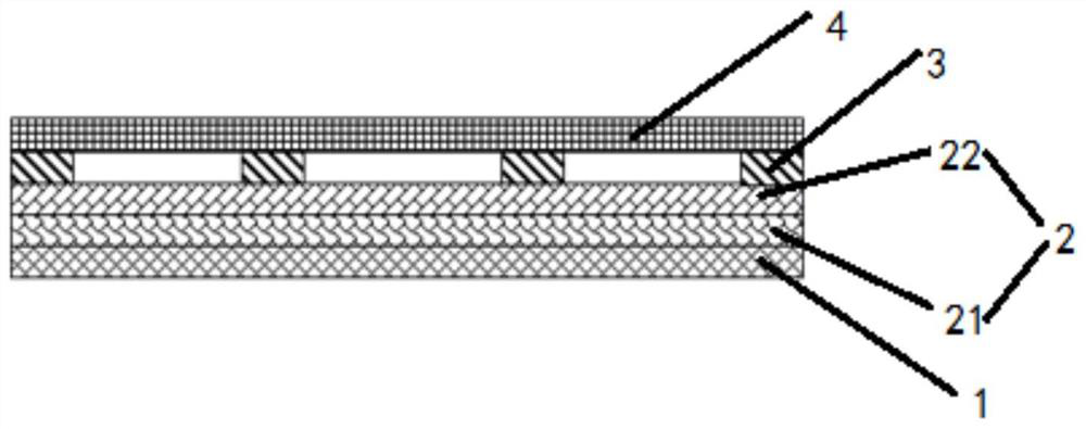
[0040] see figure 1 , is a schematic structural view of an embodiment of a graphene-based high-emissivity infrared emission film of the present invention. Specifically, the infrared emitting film of this embodiment includes a transparent substrate 1 , a graphene composite layer 2 , an electrode layer 3 and an encapsulation layer 4 which are sequentially stacked from bottom to top.
[0041]In this embodiment, the graphene composite layer 2 includes an adhesive layer 21 and a graphene layer 22, wherein the graphene layer 22 is grown on a roughened catalytic substrate by CVD, and The prepared graphene layer is transferred to the transparent substrate 1 through a liquid adhesive, thereby obtaining a graphene composite layer 2 composed of the graphene layer 22 and an adhesive layer 21 formed by curing the liquid adhesive. , and during the curing process of the adhesive layer 21 forming the graphene composite layer 2, the rough texture on the catalytic substrate is completely repro...
Embodiment 2
[0049] In order to more clearly illustrate the structure of a graphene-based high-emissivity infrared emission film of the present invention, a detailed description will be given below in conjunction with its preparation method. see Figure 4 , is a flowchart of an embodiment of a method for preparing a graphene-based high-emissivity infrared emission film of the present invention, specifically, it includes steps:
[0050] S11, roughening the growth substrate / catalytic substrate.
[0051] In this embodiment, the growth substrate (that is, the catalytic substrate) is copper foil, and the copper foil can be roughened by high temperature annealing treatment, physical mechanical polishing, chemical selective etching and other methods. In a specific embodiment, the copper foil is roughened by high-temperature annealing treatment combined with chemical micro-etching, and the step of roughening the growth substrate specifically includes the steps:
[0052] I. Under the vacuum condi...
Embodiment 3
[0069] The preparation method of this graphene-based high-emissivity infrared emission film in the present embodiment comprises each step in the above-mentioned embodiment two, and identical step adopts identical reference sign, does not repeat them here, but difference is:
[0070] In this embodiment, when the high-temperature annealing method combined with the chemical micro-etching method is used to roughen the copper foil, the substrate copper foil is heated to 950°C in the growth chamber under a vacuum condition of 150Pa, and the Protective gas, continue heating for 30min; raise the temperature of the substrate copper foil to the annealing temperature of 1080°C, and reduce the vacuum to 50Pa, and continue annealing for 10min; then, immerse the annealed substrate copper foil in a sulfuric acid / hydrogen peroxide solution with a concentration of 2wt% , etch at room temperature for 10 minutes, then wash and dry to obtain a roughened growth substrate.
[0071] The average roug...
PUM
| Property | Measurement | Unit |
|---|---|---|
| surface roughness | aaaaa | aaaaa |
| surface roughness | aaaaa | aaaaa |
| mean roughness | aaaaa | aaaaa |
Abstract
Description
Claims
Application Information


