GaN/Si heterojunction lateral light-operated IMPATT diode and preparation method thereof

A heterojunction and diode technology, used in semiconductor/solid-state device manufacturing, electrical components, circuits, etc., can solve the problem of difficult to keep up with the positive and negative conversion of high-frequency AC test signals, and achieve the effect of changing transportation

Active Publication Date: 2019-04-16
WENZHOU UNIVERSITY
View PDF5 Cites 2 Cited by
  • Summary
  • Abstract
  • Description
  • Claims
  • Application Information

AI Technical Summary

Problems solved by technology

300~330K, 0~-3V range 1~10kHz capacitance-voltage (C-V) relationship reflects the existence of negative differential capacitance (NDC), high reverse voltage, GaN / Si heterojunction conduction band quantum well energy level Far above the quasi-Fermi energy level, the quantum well state is not occupied, and the C-V relationship shows classical behavior; at low reverse voltage, the low-frequency test signal can charge and discharge the higher quantized energy level of the heterojunction conduction band quantum well , this quantum well state is occupied by charged electrons, and the C-V relationship shows NDC behavior, which can be attributed to the quantum confinement effect; however, it is difficult for the quantized energy level to charge and discharge for a long time (electron capture / escape) to keep up with the positive and negative of the high-frequency AC test signal Conversion, C-V relationship shows classical behavior
[0004] Recently Aritra Acharyya et al. compared the performance of Si and GaN homojunction collision avalanche transit time diodes [Aritra Acharyya, et al, Journal of Computational Electronics, 2015, 14:309-320.], but there is no GaN / Si heterojunction The Report of Mass Junction Lateral Light Controlled IMPATT Diode

Method used


Image

  • GaN/Si heterojunction lateral light-operated IMPATT diode and preparation method thereof
  • GaN/Si heterojunction lateral light-operated IMPATT diode and preparation method thereof
  • GaN/Si heterojunction lateral light-operated IMPATT diode and preparation method thereof

Examples


Embodiment Construction

[0043] In order to make the object, technical solution and advantages of the present invention clearer, the present invention will be further described in detail below in conjunction with the accompanying drawings and embodiments. It should be understood that the specific embodiments described here are only used to explain the present invention, not to limit the present invention.

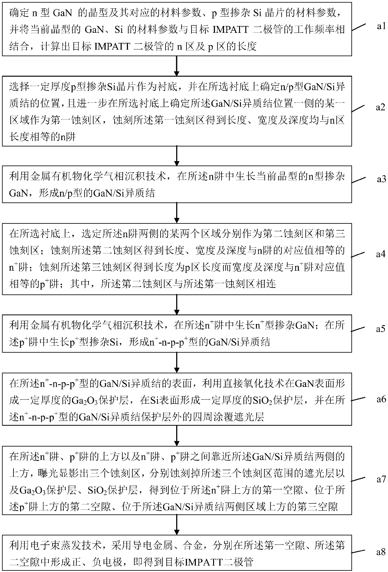
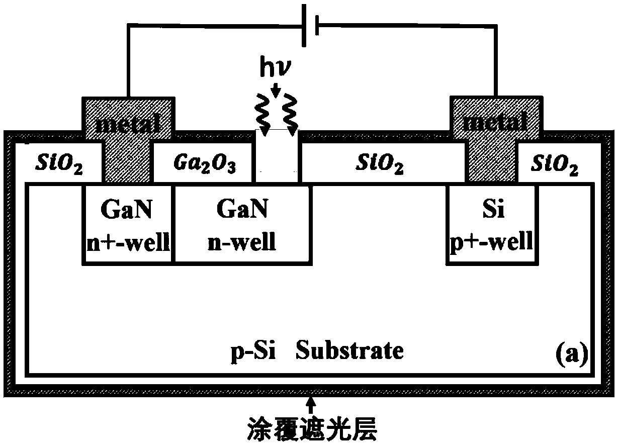
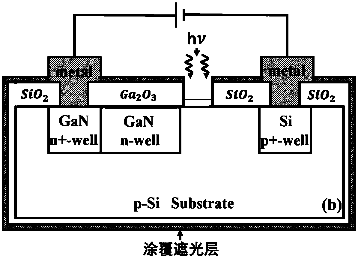
[0044] Such as figure 1 As shown, it is a GaN / Si heterojunction lateral type light-controlled IMPATT diode preparation method provided in Embodiment 1 of the present invention, which shows the (n)GaN / (p)Si heterojunction lateral The preparation method flow chart of type light control IMPATT diode specifically comprises the following steps:

[0045] Step a1, determine the crystal form of n-type doped GaN and its corresponding material parameters, the material parameters of p-type doped Si wafer, and combine the material parameters of GaN and Si of the current crystal form with the operating frequen...


PUM


Abstract

The invention discloses a GaN / Si heterojunction lateral light-operated IMPATT diode and a preparation method thereof. The method comprises the following steps: firstly, determining the crystal form, material parameters and p-type Si material parameters of n-type GaN, and calculating the lengths of an n region and a p region according to the working frequency of a target IMPATT diode; secondly, selecting a current crystal form (p) Si wafer as a substrate, respectively forming n +, n and p + wells on the substrate according to the lengths of the n region and the p region, and growing current crystal forms (n +) GaN, (n) GaN and (p +) Si in the corresponding wells; then, oxidizing to form a Ga2O3 and SiO2 protective layer, covering a shading layer, and respectively etching a first gap and a second gap to generate a positive electrode and a negative electrode; and finally, etching a third gap, introducing illumination to regulate and control the performance of the target IMPATT diode to obtain the target IMPATT diode. By implementing the IMPATT diode, the performance of the target IMPATT diode can be regulated and controlled by visible light and purple light.

Description

technical field [0001] The invention relates to the technical field of electronic transistors, in particular to a GaN / Si heterojunction lateral light-controlled IMPATT (Impact Avalanche and Transist-Time) diode and a preparation method thereof. Background technique [0002] The indirect bandgap semiconductor Si has made great contributions to the development of contemporary science and technology in integrated circuits, power electronic devices, etc., and the direct wide bandgap semiconductor (Al)GaN occupies an irreplaceable position in the field of optoelectronics such as blue-light ultraviolet illumination and detection. In recent years, the research on wide-bandgap semiconductor microwave devices represented by GaN, Si and diamond has made good progress. Such devices can work under the conditions of high temperature, high frequency and strong irradiation, and have excellent power performance. Researchers hope to grow GaN on low-cost and large-area Si to manufacture GaN / S...

Claims


Application Information

Patent Timeline
Patent Type & Authority Applications(China)
IPC IPC(8): H01L21/329H01L29/864H01L29/267
CPCH01L29/267H01L29/66159H01L29/864
Inventor 何明昌韦文生沈雨冰
Owner WENZHOU UNIVERSITY
Why Eureka
Try Eureka