An Active Broadband Pattern Reconfigurable Radome
A radome and dielectric layer technology, applied in the field of radomes, can solve the problems of complicated welding and regulation, narrow radome bandwidth, no broadband, etc., and achieve the effects of continuously adjustable switching state, expanding working bandwidth, and simple structure
- Summary
- Abstract
- Description
- Claims
- Application Information
AI Technical Summary
Problems solved by technology
Method used
Image
Examples
Embodiment 1
[0049]Example 1: Working in the direction map of 25GHz Reconfigurable antenna
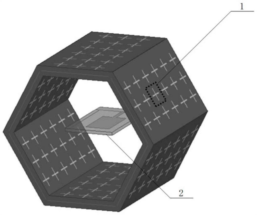
[0050]Referfigure 1 The present embodiment includes an antenna cover composed of a graphene-cross groove multilayer frequency selection surface unit 1 and a full-directional antenna 2 as a source of radiation. The frequency selection surface unit 1 consists of a pair of dielectric layers 12, a pair of dielectric layers 12, a pair of dielectric layers 12, and a center-loaded graphene patch 14.
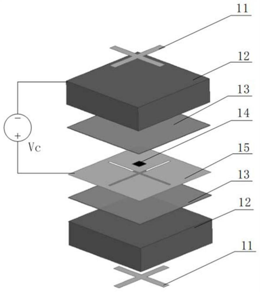
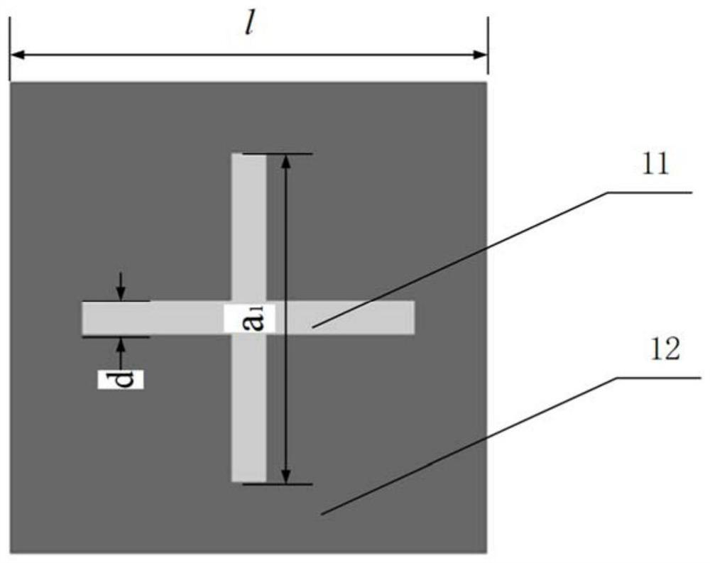
[0051]Referfigure 2 The frequency selection surface unit is a patch layer 11, the dielectric layer, the dielectric layer B 13, the graphene patch 14, the slit layer 15, the dielectric layer B 13, the dielectric layer 12, the patch layer 11 is upward The form of overlapping is made. Among them, the dielectric layer includes polysilicon, the relative dielectric constant is 11.7, the height H1 = 0.7 mm, the dielectric layer B 13 is silica, the relative dielectric constant is 3.9, the height H2 = 30 nm, and the dielectric l...
Embodiment 2
[0062]Example 2: Stepping on 22GHz Screening Reconfigurable Antenna
[0063]In this embodiment, the parameters of the full-toch patch antenna are adjusted to L = 4.3 mm, W = 2.9 mm, so that the full-to-the antenna works at 22GHz. The remaining parameters and simulation models are the same as in Example 1.
Embodiment 3
[0064]Example 3: Stepping on 28GHz Screening Reconfigurable Antenna
[0065]In this embodiment, the parameters of the full-to-pending patch antenna are adjusted to L = 3.2 mm, W = 2.0 mm, so that the whole-to-the antenna works at 28 GHz. The remaining parameters and simulation models are the same as in Example 1.
[0066]The following combined simulation calculations further describe the technical effects of the present invention:
[0067]Simulation content
[0068]1) Simulation of the graphene-metal multilayer structure frequency selection surface proposed by the present invention is simulated using HFSS full-wave simulation software.Figure 6 Indicated.
[0069]2) The antenna direction map of the first embodiment of the present invention is simulated by HFSS full-wave simulation software.Figure 7 Indicated.
[0070]3) Simulation of the antenna direction map of Example 2 of the present invention using HFSS full-wave simulation software, and the result is asFigure 8 Indicated.
[0071]4) The antenna dire...
PUM
| Property | Measurement | Unit |
|---|---|---|
| height | aaaaa | aaaaa |
| length | aaaaa | aaaaa |
| width | aaaaa | aaaaa |
Abstract
Description
Claims
Application Information


