Multi-row single-base-island lead wire framework with glue locking holes and SOT33-5L encapsulation element thereof

A lead frame and glue hole technology is used in the field of electronic device manufacturing and semiconductor packaging, which can solve the problems of increasing the resistance, inductance and parasitic capacitance of IC devices, failing to achieve good heat conduction and signal output, and reducing the efficiency of high-frequency converters. , to achieve the improvement of sealing and waterproof and moisture-proof performance, improve processability and reliability, and achieve the effect of small length

Pending Publication Date: 2019-04-23
TIANSHUI HUATIAN TECH
View PDF0 Cites 7 Cited by
  • Summary
  • Abstract
  • Description
  • Claims
  • Application Information

AI Technical Summary

Problems solved by technology

While the package shape remains unchanged, the bonding distance between the chip and the inner pins will increase, thereby increasing the internal resistance, inductance and parasitic capacitance of the IC device, reducing the performance of the high-frequency converter, and the greater the bonding distance The greater the impact, the smaller the current that can be carried, and the effect of heat conduction and signal output cannot be well realized, which greatly limits its application range

Method used


Image

  • Multi-row single-base-island lead wire framework with glue locking holes and SOT33-5L encapsulation element thereof
  • Multi-row single-base-island lead wire framework with glue locking holes and SOT33-5L encapsulation element thereof
  • Multi-row single-base-island lead wire framework with glue locking holes and SOT33-5L encapsulation element thereof

Examples


Embodiment 1

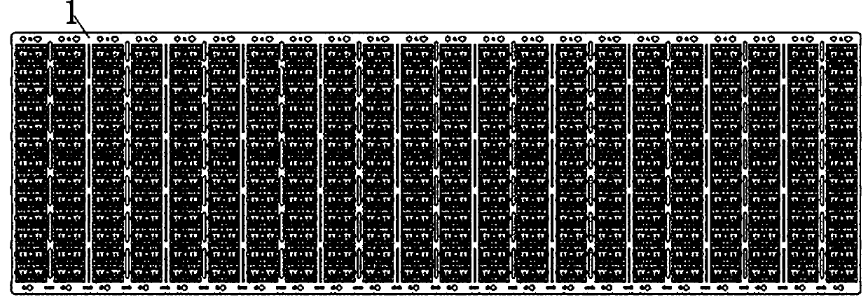
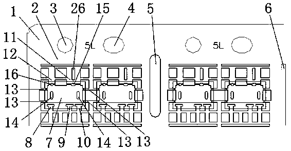
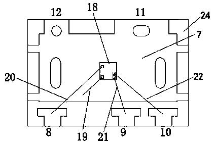
[0033] like Figure 1-2As shown, a lead frame with multiple rows of single-base islands with locking glue holes in this embodiment 1 includes a lead frame body 1 for electrically connecting the chip 18 to the external pin 25. The lead frame body 1 includes There are 13 rows and 44 columns, with a total of 572 frame units 2; the tops of lead frame units 2 in odd rows are provided with first anti-reversal holes 3, and the tops of lead frame units 2 in even rows are provided with second anti-reversal holes 4. In the present invention, every two lead frame units 2 form a group in the horizontal direction, and a process hole 5 is provided between each group of lead frame units 2 , and a first stress relief groove 6 is provided between each group of lead frame units 2 in the horizontal direction. The lead frame unit 2 includes a base island 7 whose size matches the chip 18. Five inner pins are arranged at the upper and lower ends of the base island 7, and the inner pin head and the ...

Embodiment 2

[0037] like figure 1 , Figure 5-7 As shown, the structure of a lead frame with multiple rows of single-base islands with locking glue holes in this embodiment 2 and the lead frame in embodiment 1, and the SOT33-5L package formed by using the lead frame in embodiment 2 and its implementation The difference in the structure of the package in Example 1 is that the distance between the second inner pin 9 and the third inner pin 10 is three times the distance between the first inner pin 8 and the second inner pin 9, so that The third inner pin 10 is distributed separately from the first inner pin 8 and the second inner pin 9 , so as to satisfy the package with high voltage requirements at the end of the third inner pin 10 . Other structures are with embodiment 1.

[0038] The production method of the SOT33-5L package is the same as in Embodiment 1.

Embodiment 3

[0040] like figure 1 , Figure 8-10 As shown, the difference between the structure of the lead frame with multiple rows of single-base islands with locking glue holes in Embodiment 3 and the lead frame in Embodiment 1 lies in that the fifth inner pin 12 located on the left side of the upper end of the base island 7 The head is not connected to the base island, the tail is rectangular, and its corresponding outer pin 25 is not connected to the base island 7, which can be used as an electrical output channel; the fourth inner pin and its corresponding outer pin are used as a heat dissipation channel ; Both sides of the base island are respectively provided with a first locking glue hole, and the fourth inner pin is connected with the base island to be provided with a second locking glue hole. Other structures are with embodiment 1.

[0041] The difference between the structure of the SOT33-5L package formed by using the lead frame in Embodiment 3 and the package in Embodiment ...


PUM


Abstract

The invention discloses a multi-row single-base-island lead wire framework with glue locking holes and an SOT33-5L encapsulation element thereof, and belongs to the technical field of electronic device manufacturing semiconductor encapsulation. The dimension of an arranged base island is matched with the dimension of a chip; the bonding distance of the chip and an inner lead pin is reduced; a relatively great current can be conducted; in addition, the heat generation quantity is small, so that the encapsulation requirement of chips which need relatively heavy current output can be met; meanwhile, the base island provided by the invention for carrying the chip is small; the structure is simple; the cost is low; in addition, the a wide lead pin and the base island are connected to form a heat conduction passage, so that the heat radiation of heat generation in the work process of the chip is better facilitated, so that the chip can work at a relatively low temperature. The single chip isbonded onto the base island of the lead wire framework; the glue locking holes are arranged in positions of two sides of the base islands and the connecting positions of the base islands and the inner lead pin; during the plastic encapsulation, the plastic encapsulation material penetrates through the glue locking holes, so that the firm combination of the plastic encapsulation material and the base island can be ensured; the stress can be released; the product reliability is improved.

Description

technical field [0001] The invention belongs to the technical field of semiconductor packaging for electronic device manufacturing, in particular to a lead frame with multiple rows of single-base islands with locking glue holes and its SOT33-5L package. Background technique [0002] Since the dawn of electronics manufacturing, the semiconductor industry has offered a wide variety of packages to enclose chips and provide electrical connections to semiconductor die. With the continuous development of emerging technologies such as mobile communication equipment and smart phones, semiconductor packaging is gradually tending to be high-density and miniaturized. [0003] In traditional packaging, DIP and SOP packaging are the basic packaging forms with a wide range of applications. With the development trend of integration and miniaturization in the semiconductor industry, the core component chips of semiconductors have also developed higher integration and smaller sizes. . Whil...

Claims


Application Information

Patent Timeline
Patent Type & Authority Applications(China)
IPC IPC(8): H01L23/495H01L23/31H01L23/00
CPCH01L2224/05554H01L2224/48247H01L2224/48257H01L2224/49171H01L23/4952H01L23/3114H01L23/49541H01L23/49568H01L23/562
Inventor 祁越赵萍慕蔚李琦
Owner TIANSHUI HUATIAN TECH
Why Eureka
Try Eureka