
High-temperature-resistance composite transparent conducting film and preparation method thereof

A transparent conductive film, high temperature resistant technology, applied to conductive layers on insulating carriers, equipment for manufacturing conductive/semi-conductive layers, cable/conductor manufacturing, etc. The conductive film has problems such as poor conductivity and failure, and achieves the effects of good conductivity, excellent light transmittance and low cost

Active Publication Date: 2019-04-26
SHANDONG JINJING SCIENCE & TECHNOLOGY STOCK CO LTD
View PDF3 Cites 5 Cited by
  • Summary
  • Abstract
  • Description
  • Claims
  • Application Information

AI Technical Summary

Problems solved by technology

At present, the transparent conductive film with DMD structure is easy to deteriorate or even fail due to the oxidation of the metal layer in the subsequent processing process.
Moreover, the color of the transparent conductive film of the existing DMD structure deviates from the neutral color, which is not suitable for applications in the construction field such as smart windows.

Method used


Image

  • High-temperature-resistance composite transparent conducting film and preparation method thereof
  • High-temperature-resistance composite transparent conducting film and preparation method thereof
  • High-temperature-resistance composite transparent conducting film and preparation method thereof

Examples


Embodiment 1

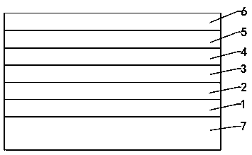
[0038] A kind of high temperature resistant and transparent composite transparent conductive film, the structure of the film layer is shown in the appendix figure 1 . Including transparent substrate 7, ion barrier layer 1 (SiNx), buffer layer 2 (SnO 2 / ITO), inner metal protective layer 3 (Ti), metal layer 4 (Ag), outer metal protective layer 5 (Ti), functional layer 6 (ZrO 2 / SiO 2 );

[0039] The thickness of the transparent substrate 7 is 3.2 mm, the thickness of the ion barrier layer 1 is 20 nm~30 nm, the thickness of the buffer layer 2 is 20~50 nm, the thickness of the Ti layer of the inner metal protection layer 3 is 0.2~1.5 nm, and the thickness of the metal layer 4 is 7 nm. ~14nm, the thickness of the Ti layer of the outer metal protective layer 5 is 0.2~1.5 nm, and the thickness of the functional layer 6 is 20~80nm;

[0040] The specific operation steps are as follows:

[0041] 1) Clean the transparent substrate 7 with a corresponding size and thickness of 3.2mm,...

Embodiment 2

[0055] The film layer structure of the composite transparent conductive film is attached figure 1 . Including transparent substrate 7, ion barrier layer 1 (SiAlNx), buffer layer 2 (ZnSnOx / ZnO), inner metal protection layer 3 (Ti), metal layer 4 (Ag), outer metal protection layer 5 (NiCr), function Layer 6 (SnO 2 / AZO / ITO / SiZrOx);

[0056] The thickness of the transparent substrate 7 is 4 mm, the thickness of the ion barrier layer 1 is 10-50 nm, the thickness of the buffer layer 2 is 20-50 nm, the thickness of the inner metal protective layer 3 is 0.2-1.5 nm, and the thickness of the metal layer 4 is 7-14 nm , The thickness of the outer metal protection layer 5 is 0.2~1.5nm, and the thickness of the functional layer 6 is 20~80nm;

[0057] The specific operation steps are as follows:

[0058] 1) Clean the transparent substrate 7 with a thickness of 4mm of the corresponding size, and set the vacuum degree of the offline magnetron sputtering equipment at 10 -3 Pa, the line s...

Embodiment 3

[0070] See the attached film structure figure 1 . Including transparent substrate 7, ion barrier layer 1 (BiOx), buffer layer 2 (SnO2 / AZO), inner metal protection layer 3 (TiV), metal layer 4 (AgCu), outer metal protection layer titanium 5 (Ti), Functional layer 6 (AZO / ITO / TiO 2 ).

[0071] The transparent substrate 7 has a thickness of 3.2 mm, the ion barrier layer 1 has a thickness of 10-20 nm, the buffer layer 2 has a thickness of 20-80 nm, the inner metal protective layer 3 has a thickness of 0.2-0.9 nm, and the metal layer 4 has a thickness of 7-14 nm. The outer metal protective layer 5 has a thickness of 0.5-1.2 nm, and the functional layer 6 has a thickness of 20-80 nm;

[0072] The specific operation steps are as follows:

[0073] 1) Clean the ultra-white transparent substrate 7 with a thickness of 3.2mm of the corresponding size, and set the vacuum degree of the offline magnetron sputtering equipment at 10 -3 Pa, the line speed is set to 4.0 m / min;

[0074] 2) ...


PUM

PropertyMeasurementUnit
Thicknessaaaaaaaaaa
Thicknessaaaaaaaaaa
Thicknessaaaaaaaaaa

Abstract

The invention provides a high-temperature-resistance composite transparent conducting film and a preparation method thereof, and belongs to the technical field of conducting films. The high-temperature-resistance composite transparent conducting film is characterized in that an ion barrier layer (1), a buffer layer (2), an inner-layer metal protecting layer (3), a metal layer (4), an outer-layer metal protecting layer (5) and a functional layer (6) are sequentially arranged on the upper surface of a transparent base plate (7) from inside to outside, so that a layered structure is formed; the inner-layer metal protecting layer (3) and the outer-layer metal protecting layer (5) are each prepared from Ti, Cu, Al, Ni, Nb, V, Cr, nickel-chromium-vanadium alloy, vanadium-titanium alloy, aluminum-titanium alloy, aluminum-nickel alloy, nickel-chromium alloy, aluminum-vanadium alloy or copper-chromium alloy. The thickness of the inner-layer metal protecting layer (3) and the outer-layer metal protecting layer (5) is 0.2nm to 1.5nm. The layers are prepared on the transparent base plate in sequence through a magnetron sputtering method. The conducting film can be tempered and is neutral in color permeation, low in haze and resistant to high temperature.

Description

technical field [0001] A high temperature resistant composite transparent conductive film and a preparation method thereof belong to the technical field of conductive films. Background technique [0002] Transparent conductive film (TCO) is a film with high transparency and conductive properties in the visible light range. It is mainly used in transparent electrodes in flat-panel TVs, touch screens, smart window glass, light-emitting diodes, and photovoltaic cells. [0003] Among the transparent conductive films, the most widely used one is tin-doped indium oxide film, commonly known as ITO film. According to reports, when the ITO film thickness is 366nm, the sheet resistance is about 66Ω / £. The deposition rate of ITO is very small, and it is necessary to increase the thickness of ITO in order to achieve below 10Ω / £. The color deviates from neutral and takes on a yellowish tint. In order to solve the dependence on ITO, the development of doped zinc oxide, carbon-based tra...

Claims


Application Information

Patent Timeline
IPC IPC(8): H01B5/14H01B13/00
CPCH01B5/14H01B13/0026
Inventor 范晓玲季亚林
Owner SHANDONG JINJING SCIENCE & TECHNOLOGY STOCK CO LTD
Learn More