High heat dissipation silicon-based package substrate and manufacturing method thereof and high heat dissipation package structure

A technology for encapsulating substrates and manufacturing methods, which is applied in the direction of microstructure technology, microstructure devices, semiconductor/solid-state device manufacturing, etc., which can solve problems such as increased manufacturing costs, increased size of integrated circuit chips, and reliability issues, and achieve low cost , Small size, high integration effect

Pending Publication Date: 2019-04-26
苏州锐杰微科技集团有限公司
View PDF0 Cites 2 Cited by
  • Summary
  • Abstract
  • Description
  • Claims
  • Application Information

AI Technical Summary

Problems solved by technology

However, the thermal conductivity of the PCB board is only 0.2-0.8W/m·K, it is difficult to export the heat emitted by the integrated circuit chip, and it is easy to cause reliability problems
Although a metal heat sink can be introduced into the packaging structure to solve the heat dissipatio

Method used


Image

  • High heat dissipation silicon-based package substrate and manufacturing method thereof and high heat dissipation package structure
  • High heat dissipation silicon-based package substrate and manufacturing method thereof and high heat dissipation package structure
  • High heat dissipation silicon-based package substrate and manufacturing method thereof and high heat dissipation package structure

Examples


Embodiment Construction

[0041] The technical solutions in the embodiments of the invention will be clearly and completely described below in conjunction with the accompanying drawings in the embodiments of the invention. Obviously, the described embodiments are only some, not all, embodiments of the invention. Based on the embodiments of the present invention, all other embodiments obtained by persons of ordinary skill in the art without making creative efforts fall within the protection scope of the present invention.

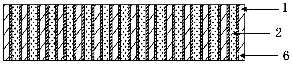
[0042] On the one hand, if figure 1 As shown, the present invention provides a high heat dissipation silicon-based packaging substrate, including a silicon substrate, the silicon substrate is longitudinally provided with a plurality of vertical through holes 9, the vertical through holes 9 run through the upper and lower surfaces of the silicon substrate, and the vertical through holes 9 Electrically conductive and thermally conductive pillars 2 are arranged inside, and both ends of ...


PUM

PropertyMeasurementUnit
Diameteraaaaaaaaaa
Resistivityaaaaaaaaaa

Abstract

The invention provides a high heat dissipation silicon-based package substrate, which includes a silicon base. A plurality of vertical through-holes are formed in the silicon base longitudinally, thevertical through-holes penetrate through the upper surface and the lower surface of the silicon base, electric and heat conducting columns are arranged in the vertical through-holes, both ends of theelectric and heat conducting columns are exposed to the upper surface and the lower surface of the silicon base, electrical isolation layers are arranged on the outer side walls of the electric and heat conducting columns, and the diameter range of the vertical through-holes is 50-200 [mu]m. The high heat dissipation silicon-based package substrate has the advantages of high heat dissipation module integration level, small volume, low cost, and being facilitated to application of a package structure. Furthermore, the invention further provides a manufacturing method of the high heat dissipation silicon-based package substrate and the package structure based on the manufacturing method.

Description

technical field [0001] The invention belongs to the technical field of packaging, and in particular relates to a silicon-based packaging substrate with high heat dissipation, a manufacturing method thereof, and a packaging structure based on the silicon-based packaging substrate with high heat dissipation. Background technique [0002] With the development of integrated circuit chips in the direction of high power consumption and high frequency, higher requirements are placed on packaging technology. Not only does the packaging structure have excellent electrical properties, it also needs to have good heat dissipation performance to ensure the long-term performance of the chip. work steadily. [0003] For the packaging of the integrated circuit chip, it is necessary to connect the integrated circuit chip to the packaging substrate to realize the electrical interconnection between the chip and the outside world. The traditional packaging substrate is prepared by PCB technolo...

Claims


Application Information

Patent Timeline
IPC IPC(8): H01L23/367H01L23/48H01L21/768
CPCH01L21/76834H01L21/76877H01L21/76898H01L23/367H01L23/481H01L2224/05553H01L2224/73265B81B2207/096B81B7/0006H01L23/147H01L23/3677H01L23/49827H01L21/4871
Inventor 孙海燕葛明敏赵继聪黄静孙玲方家恩彭一弘
Owner 苏州锐杰微科技集团有限公司
Why Eureka
Try Eureka