High-density phase change memory and preparation method thereof
Active Publication Date: 2019-04-26
SHANGHAI INTEGRATED CIRCUIT RES & DEV CENT
View PDF15 Cites 6 Cited by
Summary
Abstract
Description
Claims
Application Information
AI Technical Summary
This helps you quickly interpret patents by identifying the three key elements:
Problems solved by technology
Method used
Benefits of technology
Problems solved by technology
However, the general traditional diode drive current is not large enough to meet the operating current requirements of the phase change unit, and the manufacturing process is complicated
Method used
Image
Click on the blue label to locate the original text in one second.
Reading with bidirectional positioning of images and text.
Examples
Embodiment 1
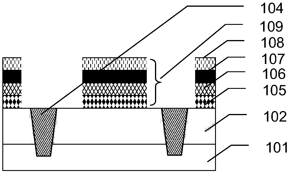
[0045] In the following specific embodiments of the present invention, please refer to figure 1 ,figure 1 It is a schematic structural diagram of a high-density phase-change memory according to the preferred embodiment 1 of the present invention. Such as figure 1 As shown, a high-density phase-change memory of the present invention includes: Schottky diodes 105 and 106 , a phase-change layer 107 and an upper electrode 108 from bottom to top. Wherein, the Schottky diode includes a semiconductor layer 105 and a metal layer 106 capable of forming a Schottky barrier with the semiconductor layer 105 ; the metal layer 106 also serves as a lower electrode of the phase change layer 107 .
[0046] The high densityphase change memory of the present invention can be disposed on a semiconductor substrate 101 . The semiconductor layer 105, the metal layer 106, the phase change layer 107 and the upper electrode 108 have a flat layer structure stacked from bottom to top.
[0047] In this...
Embodiment 2
[0054] Please refer to Figure 2-Figure 7 , Figure 2-Figure 7 is prepared figure 1 A schematic diagram of the process steps of a high-density phase-change memory. Such as Figure 2-Figure 7 As shown, a method for preparing a high-density phase-change memory of the present invention can be used to prepare a high-density phase-change memory in the first embodiment above, and may include the following steps:
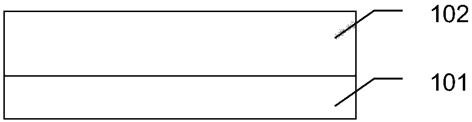
[0055] Step S01: providing a P-type semiconductor substrate, and forming an N-type heavily doped layer on the surface of the P-type semiconductor substrate.
[0056] Such as figure 2 As shown, a conventional P-type Si substrate 101 can be used, and an N-type heavily doped layer 102 is formed on the surface of the P-type Si substrate 101 by ion implantation. In this embodiment, the injection element may be As.
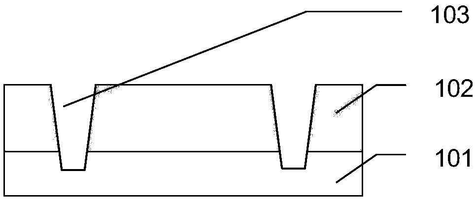
[0058] Such as image 3 As shown, a groove 103 is formed on the ...
Embodiment 3
[0068] Please refer to Figure 8 , Figure 8 It is a schematic structural diagram of a high-density phase-change memory according to the second preferred embodiment of the present invention. Such as Figure 8 As shown, a high-density phase-change memory of the present invention includes: Schottky diodes 205 and 208 , a phase-change layer 211 and an upper electrode 212 from bottom to top. The Schottky diode includes a semiconductor layer 205 and a metal layer 208 capable of forming a Schottky barrier with the semiconductor layer. The metal layer 208 also serves as the bottom electrode of the phase change layer.
[0069] Different from Embodiment 1, in this embodiment, the high-density phase-change memory can be arranged on a semiconductor substrate 201; the semiconductor layer 205, the phase-change layer 211 and the upper electrode 212 are planar structures arranged from bottom to top, The metal layer 208 is connected with a planar bottom surface and vertical sidewalls, tha...
PUM
Abstract
The invention discloses a high-density phase change memory including a Schottky diode, a phase change layer and an upper electrode from bottom to top. The Schottky diode includes a semiconductor layerand a metal layer forming a Schottky barrier with the semiconductor layer. The metal layer serves as a lower electrode of the phase change layer at the same time. The semiconductor layer, the metal layer, the phase change layer and the upper electrode are of a flat layer structure stacked from bottom to top, or the semiconductor layer, the phase change layer and the upper electrode are of a planar structure arranged from bottom to top, the metal layer is connected with a planar bottom surface and a vertical sidewall, the metal layer is overlapped with the semiconductor layer below the metal layer through the bottom surface and is connected to the phase change layer above the metal layer through the sidewall, and the phase change layer is stacked on the upper electrode. The memory can effectively improve the density of phase change memory units, reduce the number of lithography, simplify the process and reduce the manufacturing cost. The invention also discloses a preparation method ofthe high-density phase change memory.
Description
technical field [0001] The invention relates to the technical field of semiconductor integrated circuitmanufacturing technology, and more specifically, to a high-density phase-change memory and a preparation method thereof. Background technique [0002] With the emergence of a series of new information technologies such as big data, Internet of Things, cloud computing, and mobile Internet, the requirements for high read / write speed, low power consumption, high storage density, long service life, and high reliability have been put forward for memory. At present, the storage method of memory is mainly DRAM+Flash. NAND Flash has high integration and low cost, but its speed is slow and its lifespan is short. Although DRAM is fast and has a long lifespan, it loses data after power failure and is expensive. Therefore, the research and development of a new type of storage technology has become a research hotspot in the industry in recent years. This type of new storage technology...
Claims
Application Information
Patent Timeline
Application Date:The date an application was filed.
Publication Date:The date a patent or application was officially published.
First Publication Date:The earliest publication date of a patent with the same application number.
Issue Date:Publication date of the patent grant document.
PCT Entry Date:The Entry date of PCT National Phase.
Estimated Expiry Date:The statutory expiry date of a patent right according to the Patent Law, and it is the longest term of protection that the patent right can achieve without the termination of the patent right due to other reasons(Term extension factor has been taken into account ).
Invalid Date:Actual expiry date is based on effective date or publication date of legal transaction data of invalid patent.

