Method for manufacturing field effect transistor and semiconductor device

A manufacturing method and technology of field effect transistors, which are applied in semiconductor/solid-state device manufacturing, electrical components, circuits, etc., can solve problems such as insufficient gate control capability and short channel effect, reduce short channel effect, and improve gate control. capacity and carrier concentration, and the effect of improving performance

Active Publication Date: 2020-12-11
SHANGHAI INTEGRATED CIRCUIT RES & DEV CENT
View PDF4 Cites 0 Cited by
  • Summary
  • Abstract
  • Description
  • Claims
  • Application Information

AI Technical Summary

Problems solved by technology

Therefore, from planar CMOS devices to three-dimensional FinFET devices, the size of field effect transistors has been continuously reduced, the power consumption area ratio has been greatly reduced, and the device performance has been greatly improved, but at the same time problems such as insufficient gate control capabilities and serious short channel effects have appeared. , has a great influence on the performance of the device
[0003] Therefore, in order to solve the problems of insufficient gate control capability and serious short channel effect accompanying the reduction of the size of field effect transistors, a new method for manufacturing field effect transistors and semiconductor devices is needed

Method used


Image

  • Method for manufacturing field effect transistor and semiconductor device
  • Method for manufacturing field effect transistor and semiconductor device
  • Method for manufacturing field effect transistor and semiconductor device

Examples


Embodiment Construction

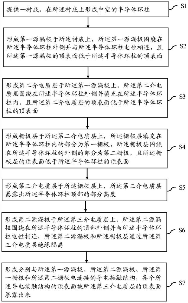
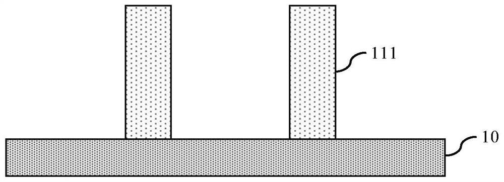
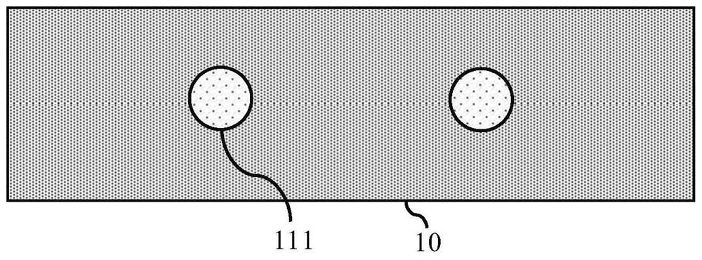
[0034] In order to make the purpose, advantages and characteristics of the present invention clearer, the following in conjunction with the attached Figure 1~2o' The manufacturing method of the field effect transistor and the semiconductor device proposed by the present invention will be further described in detail. It should be noted that all the drawings are in a very simplified form and use imprecise scales, and are only used to facilitate and clearly assist the purpose of illustrating the embodiments of the present invention.

[0035] An embodiment of the present invention provides a method for manufacturing a field effect transistor, see figure 1 , figure 1 It is a flowchart of a method for manufacturing a field effect transistor according to an embodiment of the present invention, and the method for manufacturing a field effect transistor includes:

[0036] Step S1, providing a substrate, and forming a hollow semiconductor ring pillar on the substrate;

[0037] Step ...


PUM


Abstract

The invention provides manufacturing methods for a field-effect transistor and a semiconductor device. The manufacturing method for the field-effect transistor includes the following steps: forming hollow semiconductor ring columns on a substrate; forming a first source drain electrode on the substrate; forming a second dielectric substance layer on the first source drain electrode; forming firstgrid electrodes filled in the semiconductor ring columns and second grid electrodes surrounding outsides of the semiconductor ring columns; forming a third dielectric substance layer on a grid electrode layer; forming a second source drain electrode on the third dielectric substance layer; and forming a conductive contact structure separately electrically connected to the first source drain electrode, the second source drain electrode, the first grid electrodes, and the second grid electrodes. According to the technical scheme provided by the manufacturing methods, dual control of electric fields in the semiconductor ring columns is achieved, so that while the size of the field-effect transistor is reduced, and grid control capability and carrier concentration of the field-effect transistor can also be improved, a short-channel effect is reduced, thereby improving the performance of the semiconductor device.

Description

technical field [0001] The invention relates to the field of semiconductor integrated circuit manufacturing, in particular to a method for manufacturing a field effect transistor and a semiconductor device. Background technique [0002] Field Effect Transistor (FET) is a voltage-controlled semiconductor device. According to Moore's Law, the size of Field Effect Transistor is continuously shrinking. After reaching the 40nm process node, planar CMOS devices have insufficient gate control capability, short Problems such as serious channel effects cannot meet the requirements of the industry. At this time, the developed three-dimensional device fin field effect transistor (FinFET) improves the gate control capability through three-sided gate control and reduces the short channel effect. When the semiconductor develops to the 7nm process node, the channel length is shortened to less than 20nm, and the quantum effect of semiconductor material transport gradually becomes prominent....

Claims


Application Information

Patent Timeline
Patent Type & Authority Patents(China)
IPC IPC(8): H01L21/285H01L21/336
Inventor 尚恩明胡少坚陈寿面
Owner SHANGHAI INTEGRATED CIRCUIT RES & DEV CENT
Why Eureka
Try Eureka