
Passivated solar cell with printed metal electrodes and preparation method thereof

A solar cell and metal electrode technology, which is applied in the field of solar cells, can solve the problems of not considering the recombination of metal and semiconductor contact areas and affecting the efficiency of crystalline silicon solar cells, so as to reduce metal contact recombination and resistance loss, improve open circuit voltage and Conversion efficiency, effect of increasing depth

Pending Publication Date: 2019-05-03
TAIZHOU ZHONGLAI PHOTOELECTRIC TECH CO LTD
View PDF12 Cites 10 Cited by
  • Summary
  • Abstract
  • Description
  • Claims
  • Application Information

AI Technical Summary

Problems solved by technology

[0005] The above-mentioned patent uses the silver paste to burn through the silicon oxide film and silicon nitride film to contact the silicon substrate, but it does not consider the serious recombination of the metal and semiconductor contact area, which seriously affects the efficiency of crystalline silicon solar cells.

Method used


Image

  • Passivated solar cell with printed metal electrodes and preparation method thereof
  • Passivated solar cell with printed metal electrodes and preparation method thereof
  • Passivated solar cell with printed metal electrodes and preparation method thereof

Examples


Embodiment Construction

[0042] The present invention will be described in detail below in conjunction with the embodiments and the accompanying drawings. It should be noted that the described embodiments are only intended to facilitate the understanding of the present invention, rather than limiting it in any way.

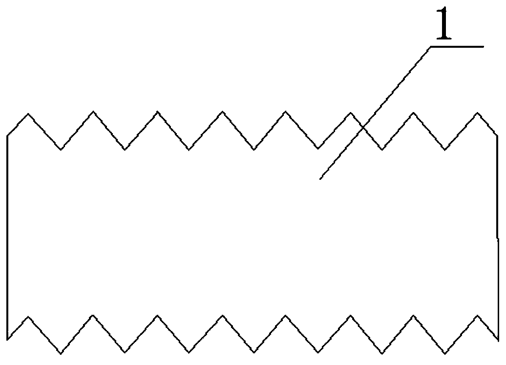
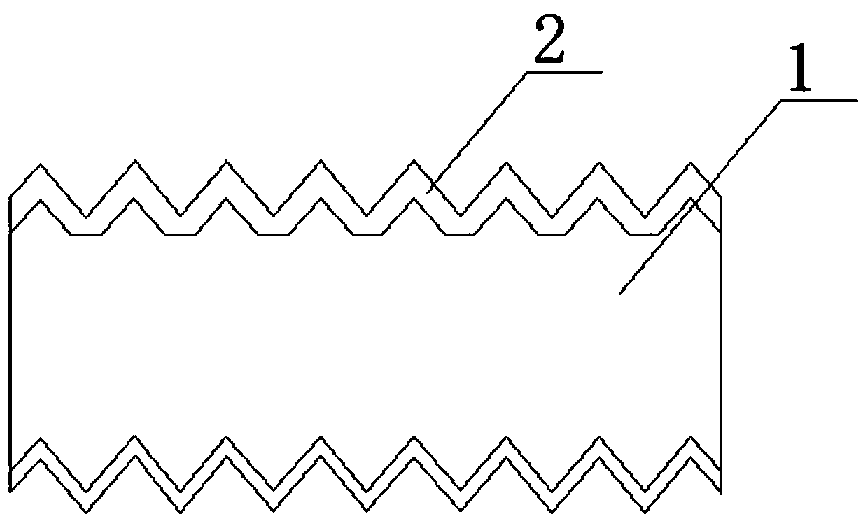
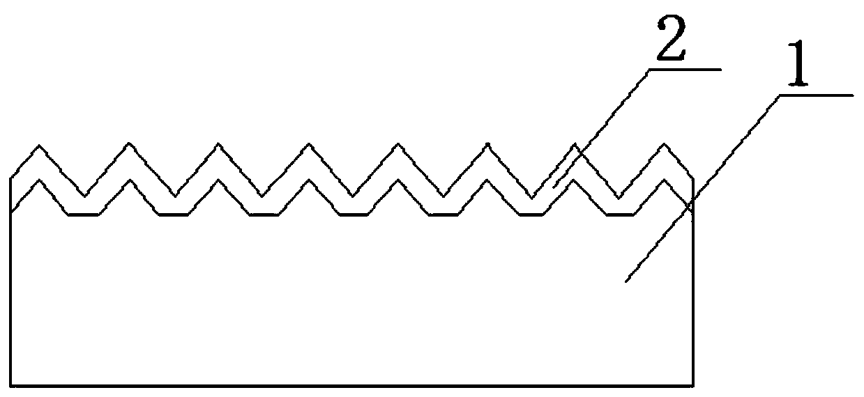
[0043]A passivated solar cell with printed metal electrodes in this embodiment includes an N-type crystalline silicon substrate 1, the back surface of the N-type crystalline silicon substrate 1 sequentially includes an n+ doped polysilicon layer 5, a back passivation antireflection Thin film 7, n+ metal electrode 9;

[0044] A doped polysilicon tail layer 6 is formed on the side of the N-type crystalline silicon substrate 1 close to the n+ doped polysilicon layer 5 .

[0045] The band tail of polysilicon doping, that is, the depth to which dopant atoms diffuse in crystalline silicon, plays a decisive role in the size of metal contact recombination. The research results show that the thic...


PUM

PropertyMeasurementUnit
thicknessaaaaaaaaaa
thicknessaaaaaaaaaa
thicknessaaaaaaaaaa

Abstract

The invention relates to a passivated solar cell with printed metal electrodes and a preparation method thereof. The passivated solar cell comprises an N-type crystalline silicon substrate, and the back surface of the N-type crystalline silicon substrate sequentially comprises an n+ doped polycrystalline silicon layer, a back passivated antireflection film and n+ metal electrodes from inside to outside. A doped polycrystalline silicon band tail layer is formed at one side, close to the n+ doped polycrystalline silicon layer, of the N-type crystalline silicon substrate. The band tail of the doped polycrystalline silicon layer in the metal contact region is prolonged, and the diffusion depth of doped atoms in crystalline silicon is increased, thereby reducing the recombination of the metal contact region. The band tail of the doped polycrystalline silicon layer in the non-metal contact region remains shallower, and the recombination of the non-metal contact region is reduced. The methodis simple in process, and the n+ doped polycrystalline silicon layers of the first region and the second region can be completed through one-time doping. The related technological processes are industrialized and suitable for large-scale production. Metal contact recombination and resistance loss can be obviously reduced, and open-circuit voltage and conversion efficiency of the cell are improved.

Description

technical field [0001] The invention relates to the technical field of solar cells, in particular to a passivated solar cell with printed metal electrodes and a preparation method thereof. Background technique [0002] At present, the most commonly used metallization method in the industrialization of crystalline silicon solar cells is screen printing and sintering. The screen printing and sintering process will make the metal penetrate through the oxide layer and the doped polysilicon layer, and directly contact the silicon substrate. , resulting in a surge of recombination under the metal region, causing a large recombination loss. Especially for the paste using silver-aluminum paste, the phenomenon that the metal penetrates the oxide layer and the doped polysilicon layer will be more serious. [0003] In crystalline silicon solar cells, the severe recombination of metal and semiconductor contact regions has become an important factor restricting the development of crysta...

Claims


Application Information

Patent Timeline
Patent Type & Authority Applications(China)
IPC IPC(8): H01L31/0352H01L31/0368H01L31/068H01L31/18
CPCY02E10/546Y02P70/50
Inventor 林建伟包杰吴伟梁刘志锋陈嘉吴兴华
Owner TAIZHOU ZHONGLAI PHOTOELECTRIC TECH CO LTD
Learn More