Check patentability & draft patents in minutes with Patsnap Eureka AI!

Semiconductor structure and manufacturing method thereof

A manufacturing method and semiconductor technology, applied in semiconductor/solid-state device manufacturing, semiconductor devices, semiconductor/solid-state device components, etc., can solve problems such as increasing the cost of semiconductor device manufacturing processes, and achieve the effect of ensuring yield

Active Publication Date: 2019-05-07
SHANGHAI HUALI INTEGRATED CIRCUTE MFG CO LTD
View PDF7 Cites 1 Cited by
  • Summary
  • Abstract
  • Description
  • Claims
  • Application Information

AI Technical Summary

Problems solved by technology

However, due to the particularity of the position of the Kelvin via, which is located in the turning area, unauthorized modification of the characteristic size of the Kelvin via requires a large number of changes to the layout design of the entire semiconductor device, which increases the cost of the semiconductor device manufacturing process

Method used


Image

  • Semiconductor structure and manufacturing method thereof
  • Semiconductor structure and manufacturing method thereof
  • Semiconductor structure and manufacturing method thereof

Examples


Embodiment Construction

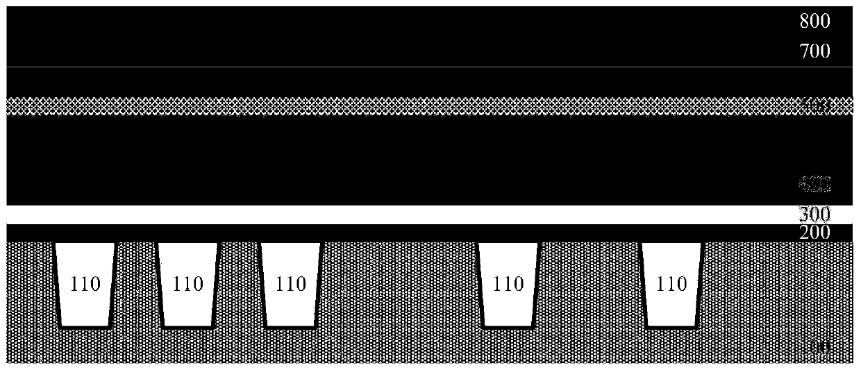
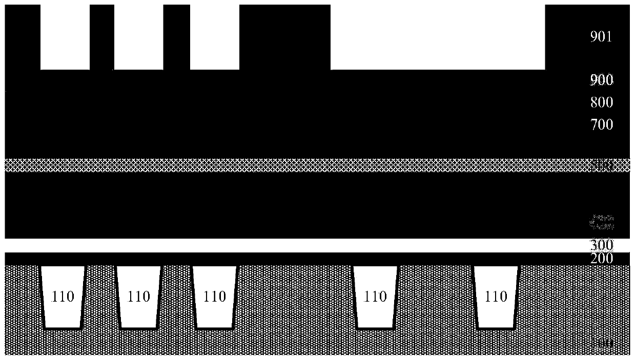
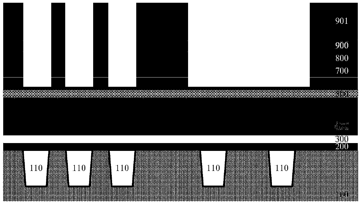
[0048] The following description is given to enable a person skilled in the art to make and use the invention and incorporate it into a specific application context. Various modifications, and various uses in different applications will be readily apparent to those skilled in the art, and the general principles defined herein may be applied to a wide range of embodiments. Thus, the present invention is not limited to the embodiments given herein but is to be accorded the widest scope consistent with the principles and novel features disclosed herein.

[0049] In the following detailed description, numerous specific details are set forth in order to provide a better understanding of the present invention. It will be apparent, however, to one skilled in the art that the practice of the present invention need not be limited to these specific details. In other words, well-known structures and devices are shown in block diagram form and not in detail in order to avoid obscuring th...


PUM


Abstract

The present invention provides a semiconductor structure and a manufacturing method thereof. The semiconductor structure includes a through hole penetrating through a dielectric layer in a height direction of the semiconductor structure. The through hole interconnects the front device of the semiconductor structure with the rear metal line of the semiconductor structure. By performing a first etching process and a second etching process, the cross section of the formed through hole orthogonal to the height direction has a first dimension in the extending direction of the rear metal line greater than a second dimension in the direction perpendicular to the extending direction. According to the through hole structure formed by the manufacturing method provided by the present invention, the feature size of the through hole in the second direction is unchanged and the feature size of the through hole in the first direction can be increased when a photomask is not modified, thereby reducingthe resistance value of a metal contact located in the through hole, and avoiding a short circuit in the second direction.

Description

technical field [0001] The invention relates to a semiconductor structure and a manufacturing method thereof, in particular to designing a through-hole structure and a manufacturing method thereof. Background technique [0002] Since the early days when Dr. Jack Kilby of Texas Instruments invented the integrated circuit, scientists and engineers have made numerous inventions and improvements in semiconductor devices and processes. Over the past 50 years, there has been a significant reduction in the size of semiconductors, which translates into ever-increasing processing speeds and ever-decreasing power consumption. So far, the development of semiconductors has roughly followed Moore's Law, which roughly states that the number of transistors in a dense integrated circuit doubles about every two years. Now, the semiconductor process is developing below 28nm, and some companies are working on the 14nm process. Here is just a reference, a silicon atom is about 0.2nm, which me...

Claims


Application Information

Patent Timeline
IPC IPC(8): H01L21/768H01L23/522H01L23/528
Inventor 张年亨
Owner SHANGHAI HUALI INTEGRATED CIRCUTE MFG CO LTD
Features
  • R&D
  • Intellectual Property
  • Life Sciences
  • Materials
  • Tech Scout
  • Unparalleled Data Quality
  • Higher Quality Content
  • 60% Fewer Hallucinations
Learn More