
All-inorganic white light LED packaging structure and preparation method thereof

A technology of LED packaging and LED chips, which is applied in the direction of semiconductor devices, electrical components, circuits, etc., can solve the problems that affect the long-term reliability of white light LEDs, it is difficult to meet the lighting requirements, and the aging of organic materials, so as to avoid aging and failure problems. Improve packaging efficiency and integration, and avoid thermal damage

Inactive Publication Date: 2019-05-07
HUAZHONG UNIV OF SCI & TECH
View PDF4 Cites 8 Cited by
  • Summary
  • Abstract
  • Description
  • Claims
  • Application Information

AI Technical Summary

Problems solved by technology

[0004] The existing fluorescent glass packaging forms still inevitably use organic polymers as bonding materials for the bonding between fluorescent glass and packaging substrates. This packaging form will still have organic materials under long-term heat radiation and light irradiation. Aging problems, resulting in lower transmittance, bond failure and other problems
At the same time, the existing fluorescent glass-encapsulated white light LEDs are not hermetically sealed, and water vapor and oxygen in the external environment are easy to invade the package, which seriously affects the long-term reliability of white light LEDs, making it difficult to apply to lighting requirements in harsh environments.

Method used


Image

  • All-inorganic white light LED packaging structure and preparation method thereof
  • All-inorganic white light LED packaging structure and preparation method thereof

Examples


Embodiment 1

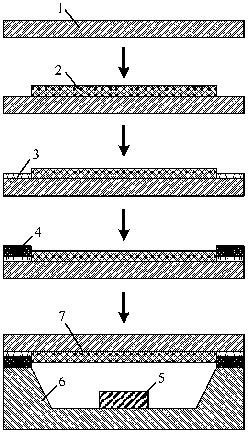
[0045] Such as figure 1 As shown, the steps of preparing the all-inorganic white LED packaging structure include:

[0046] (a) Mix 3g of terpineol and 0.15g of ethyl cellulose, and stir ultrasonically at 70°C until the ethyl cellulose is completely dissolved as a binder for the glass slurry, then add 12.6g of YAG yellow fluorescent powder and 5g of low-temperature borosilicate glass powder, and finally obtain the fluorescent glass slurry by magnetic stirring for 15 minutes; choose ordinary soda-lime glass as the substrate, and coat a layer of uniform thickness on one side of the glass sheet 1 by screen printing. The fluorescent glass paste is then placed in a high-temperature furnace, heated and sintered at 600° C. for 30 minutes to form a fluorescent glass layer 2 with a thickness of 90 μm;

[0047] (b) printing a layer of nano-silver paste around the fluorescent glass layer 2 obtained in step (a), and forming a sintered silver layer with uniform thickness by low-temperature...

Embodiment 2

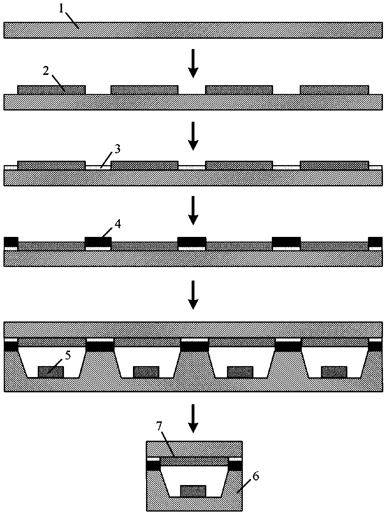
[0051] Such as figure 2 As shown, the steps of preparing the all-inorganic white LED packaging structure include:

[0052] (a) Mix 4g of terpineol and 0.2g of ethyl cellulose, and stir ultrasonically at 70°C until the ethyl cellulose is completely dissolved as a binder for the glass slurry, then add 3g of YAG yellow fluorescent powder, 1g of CASN red fluorescent powder and 6g of low-temperature tellurite glass powder, and finally obtain the fluorescent glass slurry by magnetically stirring for 15 minutes; select a wafer-level quartz glass sheet as the substrate, and coat one side of the glass sheet 1 by screen printing A layer of the fluorescent glass paste with a uniform thickness is placed in a high-temperature furnace, heated and sintered at 500° C. for 60 minutes to form a fluorescent glass layer 2 with a thickness of 150 μm;

[0053] (b) On one side of the fluorescent glass layer 2 obtained in step (a), form a mask pattern by photolithography and development, and then f...

Embodiment 3

[0057] The steps of preparing the all-inorganic white LED packaging structure include:

[0058] (a) Mix 6g of terpineol and 0.4g of ethyl cellulose, and stir ultrasonically at 70°C until the ethyl cellulose is completely dissolved as a binder for the glass slurry, and then add 2.5g of YAG yellow fluorescent powder and 25.4g of low-temperature borosilicate glass powder, and finally obtain fluorescent glass slurry by magnetically stirring for 15 minutes; choose ordinary soda-lime glass as the substrate, and coat a layer of fluorescent glass with a uniform thickness on one side of the glass sheet 1 by screen printing. The glass paste is then placed in a high-temperature furnace, heated and sintered at 650° C. for 20 minutes to form a fluorescent glass layer 2 with a thickness of 30 μm;

[0059] (b) printing a layer of nano-copper paste around the fluorescent glass layer 2 obtained in step (a), and forming a sintered copper layer with uniform thickness by low-temperature sintering...


PUM

PropertyMeasurementUnit
Thicknessaaaaaaaaaa
Glass transition temperatureaaaaaaaaaa
Thicknessaaaaaaaaaa

Abstract

The invention belongs to the related technical field of semiconductor manufacturing, and specifically discloses an all-inorganic white light LED packaging structure and a preparation method thereof. The structure comprises a heat dissipation substrate, an LED chip and a fluorescent glass sheet, wherein the heat dissipation substrate includes a base and a support body, and a cavity is formed between the base and the support body; the LED chip is placed in the cavity and fixed on the base of the heat dissipation substrate; the fluorescent glass sheet is placed above the heat dissipation substrate, a fluorescent glass layer directly faces the LED chip, the periphery of the fluorescent glass fluorescent glass layer is a metal layer, a welding flux layer is processed on the metal layer, and theairtight welding between the fluorescent glass sheet and the support body of the heat dissipation substrate is realized through melting the welding flux layer. The all-inorganic white light LED packaging structure is enabled to have good thermal resistance and thermal reliability through preparing the fluorescent glass layer; and meanwhile, the aging and failure of an organic bonding material canbe avoided through the airtight welding between the fluorescent glass sheet and the heat dissipation substrate, and thus the reliability of white light LEDs is significantly improved.

Description

technical field [0001] The invention belongs to the technical field related to semiconductor manufacturing, and more specifically relates to an all-inorganic white LED packaging structure and a preparation method thereof. Background technique [0002] Compared with traditional lighting sources such as incandescent lamps and fluorescent lamps, white LEDs have the advantages of high luminous efficiency, long life, environmental protection and energy saving, and compact structure. They have been widely used in lighting, backlight display and other fields, such as indoor lighting, landscape lighting, street lights, Car headlights, TV backlights, etc. At present, blue LED chip excites yellow phosphor powder is a common method to realize white LED. The packaging form of white LED is that phosphor powder is mixed with organic polymers such as silica gel to form phosphor powder glue, which is coated on the surface of LED chip or coated far away from the chip. cover. However, due t...

Claims


Application Information

Patent Timeline
IPC IPC(8): H01L33/54H01L33/56H01L33/50H01L33/64
Inventor 彭洋牟运柳星星陈明祥罗小兵
Owner HUAZHONG UNIV OF SCI & TECH
Learn More