A kind of recessed anode plane Gunn diode and its manufacturing method

A Gunn diode and anode technology, which is applied in the field of grooved anode plane Gunn diode and its production, can solve the problems of device output power degradation, material quality reduction, and bias voltage reduction, and achieve the effect of increasing operating frequency and output power

Inactive Publication Date: 2020-09-25
NORTHWESTERN POLYTECHNICAL UNIV
View PDF5 Cites 0 Cited by
  • Summary
  • Abstract
  • Description
  • Claims
  • Application Information

AI Technical Summary

Problems solved by technology

[0004] The frequency expression of the Gunn diode is: f=v sat / L, where v sat is the electron saturation speed, and L is the channel length, so the most direct way to increase the frequency is to shorten the channel length L; however, if the channel is too short, the supported external working bias will also become lower, although the frequency is increased, But the corresponding output power is greatly reduced
In the prior art, there are two types of new structures that can improve the operating frequency and output power of Gunn devices, one is an ultra-short multi-channel structure based on multiple AlGaN (AlInN or AlN) / GaN heterojunctions, and Limited by the current technology level, as the number of channels increases, the process difficulty increases and the material quality also decreases; the other type is the harmonic enhanced structure, which improves the device structure by improving the long channel device structure. The nonlinearity of the oscillation produces higher harmonic frequencies, thereby realizing the high frequency of the Gunn device, but the higher the harmonic frequency, the output power of the device will be seriously degraded

Method used


Image

  • A kind of recessed anode plane Gunn diode and its manufacturing method
  • A kind of recessed anode plane Gunn diode and its manufacturing method
  • A kind of recessed anode plane Gunn diode and its manufacturing method

Examples


Embodiment 1

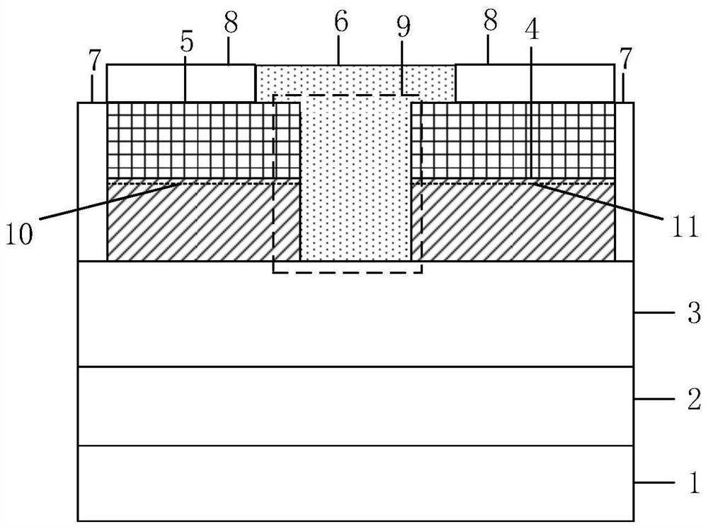
[0046] See figure 1 , figure 1 A structural schematic diagram of a grooved anode double-channel planar Gunn diode provided for an embodiment of the present invention, including: a substrate 1; a nucleation layer 2 located on the substrate 1 and a back barrier layer 3 located on the nucleation layer 2 on the channel layer 4, located on the back barrier layer 3; the barrier layer 5, located on the channel layer 4; wherein, the channel layer 4 and the barrier layer 5 are provided with a groove 9; the anode 6 is located in the concave The groove 9 is located on the back barrier layer 3 and the barrier layer 5; the cathode 7 is located on the back barrier layer 3; the dielectric layer 8 is located on the barrier layer 5.

[0047] In a specific embodiment, the material of the substrate 1 includes but not limited to diamond / sapphire / SiC / high resistance GaN, preferably, the substrate material is diamond.

[0048] In the existing research, the most important factor restricting the re...

Embodiment 2

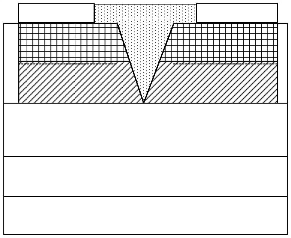
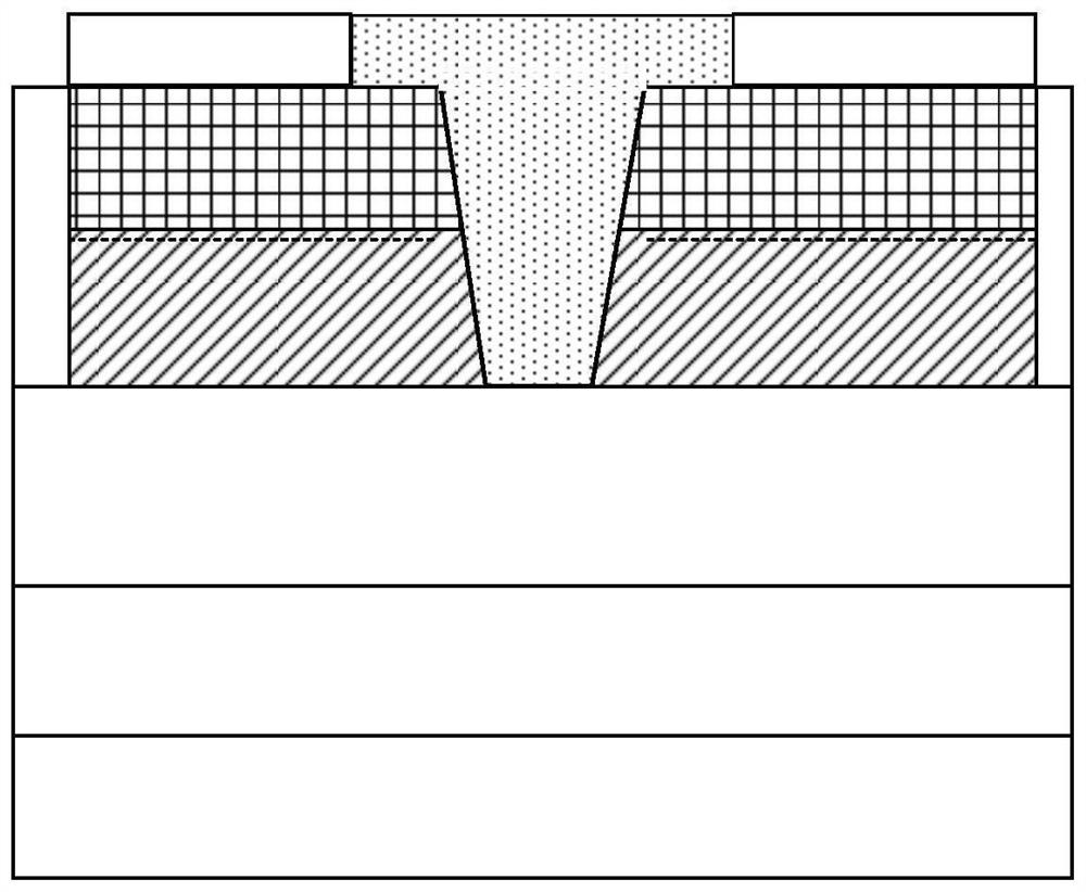
[0068] See Figure 5a-5d , Figure 5a-5d A schematic flow chart of a method for preparing a grooved anode dual-channel planar Gunn diode provided in an embodiment of the present invention, including steps:

[0069] S1. Pretreating the surface of the substrate 1 in the reaction chamber;

[0070] S2, growing nucleation layer 2, back barrier layer 3, channel layer 4 and barrier layer 5 sequentially on the substrate, see Figure 5a ;include:

[0071] S21. Using a chemical vapor deposition process (Chemical Vapor Deposition, CVD for short) or a physical vapor deposition process (Physical Vapor Deposition, PVD), grow an AlN nucleation layer 2 with a thickness of 3 nm to 3 μm on the substrate 1;

[0072] S22. Growing a back barrier layer 3 with a thickness of 100 nm to 1000 nm on the AlN nucleation layer 2 by using a CVD process or a PVD process, and the material of the back barrier layer 3 includes Al x Ga 1-x N, where, Al x Ga 1-x The N material has no intentional doping, an...

Embodiment 3

[0090] See Figure 6 , Figure 6 A grooved anode multi-channel planar Gunn diode provided for an embodiment of the present invention includes: a substrate 1; a nucleation layer 2 located on the substrate 1; a back barrier layer 3 located on the nucleation layer 2; The channel layer 64 and the barrier layer 65 are stacked alternately on the back barrier layer 3 in turn; wherein, the channel layer 64 and the barrier layer 65 are provided with a groove 9, and the groove 9 connects the channel layer 64 and the The 2DEG channel formed between the barrier layer 65 is divided into a first 2DEG channel 610 and a second 2DEG channel 611; the anode 6 is located in the groove 9 and on the barrier layer 65; the cathode 7 is located in the back barrier layer 3; the dielectric layer 8 is located on the 2DEG channel structure.

[0091] exist Figure 6 including a channel layer 641 on the back barrier layer 3, a barrier layer 651 on the channel layer 641, a channel layer 642 on the barrier...


PUM

PropertyMeasurementUnit
thicknessaaaaaaaaaa
thicknessaaaaaaaaaa
thicknessaaaaaaaaaa

Abstract

The invention relates to a grooved anode planar Gunn diode, comprising a substrate, a nucleating layer, a back barrier layer, a channel layer, a barrier layer, an anode, a cathode and a dielectric layer, wherein the nucleating layer is located on the substrate; the back barrier layer is located on the nucleating layer; the channel layer is located on the back barrier layer; the barrier layer is located on the channel layer; grooves are arranged on the barrier layer and the channel layer, and the grooves divide 2DEG channels formed by the channel layer and the barrier layer into a first 2DEG channel and a second 2DEG channel; the anode is located in the grooves and on the barrier layer; the cathode is located on the back barrier layer; and the dielectric layer is located on the barrier layer. According to the embodiment of the invention, the grooves are utilized to form two parallel planar Gunn diodes, the movement of electronic domains in the channels is changed by changing the lengthsof the two channels, the free control of the operating frequency and the output power of devices is realized, and the scheme has great significance to the research of improving the operating frequency and the output power of the devices.

Description

technical field [0001] The invention belongs to the field of semiconductors, and in particular relates to a grooved anode plane Gunn diode and a manufacturing method thereof. Background technique [0002] Gunn diode devices or electron transfer devices (TEDs) are considered to be excellent microwave and lower millimeter wave (30GHz-100GHz) signal source devices, and have been recognized by more and more people since they were first confirmed by J.B. Gunn in 1963 focus on. Compared with traditional signal source devices, such as klystrons, magnetrons, and return wave oscillators, Gunn diodes are smaller in size, simpler in structure, and lower in power consumption. In the development of more than 50 years, Gunn diode has become one of the most widely used microwave signal sources, widely used in industry, science, medical and military fields. [0003] In the study of Gunn diodes, planar Gunn devices have gradually attracted attention. Due to the strong piezoelectric polari...

Claims


Application Information

Patent Timeline
Patent Type & Authority Patents(China)
IPC IPC(8): H01L47/02H01L47/00
Inventor 汪瑛李萌敖金平张进成刘诗斌周德云郝跃
Owner NORTHWESTERN POLYTECHNICAL UNIV
Why Eureka
Try Eureka