High-reliability photoresist glass passivation chip and processing method thereof
A glass passivation and processing method technology, applied in electrical components, electrical solid devices, circuits, etc., can solve the problems of short chip service life, easy chip failure, and easy breakdown, so as to achieve long service life and reduce chip failure. risk, avoid the effect of mass aggregation
- Summary
- Abstract
- Description
- Claims
- Application Information
AI Technical Summary
Problems solved by technology
Method used
Image

Examples
Embodiment 1
[0041] A method for processing a highly reliable photoresist glass passivation chip, comprising the following steps:
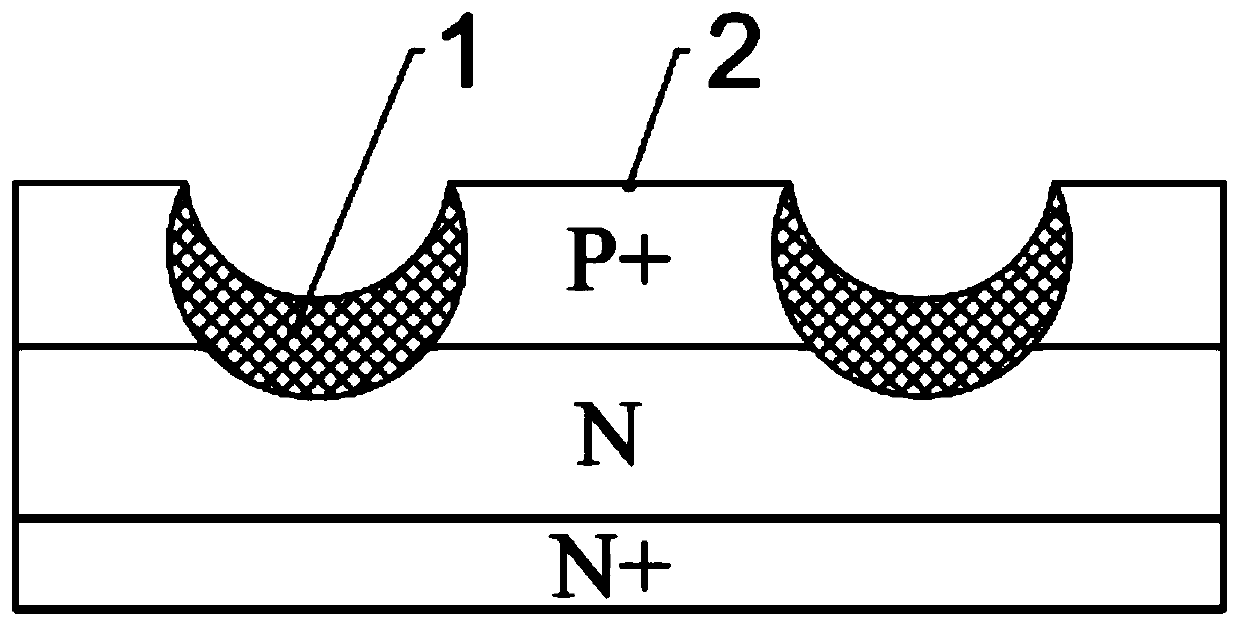
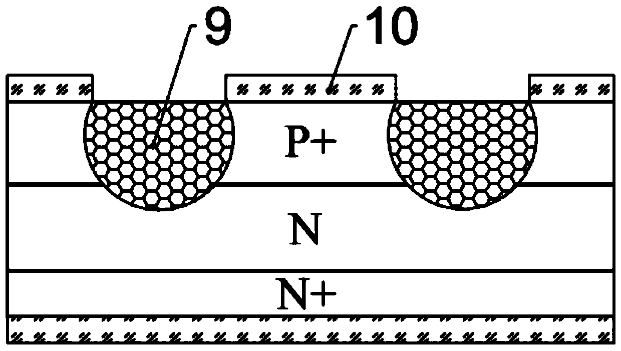
[0042] S1, one-time photolithography: apply glue, bake, expose, develop and fix on the diffused chip body, complete one-time photolithography, and form a groove corrosion area without photoresist 10 protection on the chip body;
[0043] S2. Groove etching and photoresist removal: Corrosion is carried out in a low-temperature mixed acid at -4°C, and the groove corrosion area 9 is etched to obtain a groove with a required depth, and then the photoresist on the surface of the chip body is removed;
[0044] S3. Cleaning: Clean the chip body with high-purity water, and then dry and arrange the chips with nitrogen gas. From this step, the working environment needs to reach a purification level of more than 10,000 grades;
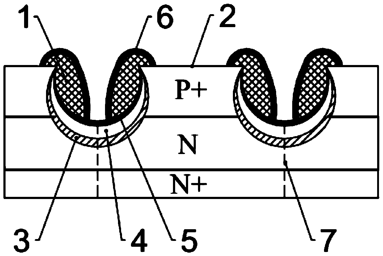
[0045] S4. Silicon atom film deposition: Deposit a layer of silicon atoms on the surface of the chip body. The silicon atoms will first fill the ...
Embodiment 2
[0056] A method for processing a highly reliable photoresist glass passivation chip, comprising the following steps:
[0057] S1, one-time photolithography: apply glue, bake, expose, develop and fix on the diffused chip body, complete one-time photolithography, and form a groove corrosion area without photoresist 10 protection on the chip body;
[0058] S2. Groove etching and photoresist removal: Corrosion is carried out in a low-temperature mixed acid at -8°C, and the groove corrosion area 9 is etched to obtain a groove with a required depth, and then the photoresist on the surface of the chip body is removed;
[0059] S3. Cleaning: Clean the chip body with high-purity water, and then dry and arrange the chips with nitrogen gas. From this step, the working environment needs to reach a purification level of more than 10,000 grades;
[0060] S4. Silicon atom thin film deposition: Deposit a layer of silicon atoms on the surface of the chip body. The silicon atoms will first fill...
Embodiment 3
[0071] A method for processing a highly reliable photoresist glass passivation chip, comprising the following steps:
[0072] S1, one-time photolithography: apply glue, bake, expose, develop and fix on the diffused chip body, complete one-time photolithography, and form a groove corrosion area without photoresist 10 protection on the chip body;
[0073] S2. Groove etching and photoresist removal: corrode in a low-temperature mixed acid at -10°C, the groove corrosion area 9 is etched to obtain a groove with a required depth, and then remove the photoresist on the surface of the chip body;
[0074] S3. Cleaning: Clean the chip body with high-purity water, and then dry and arrange the chips with nitrogen gas. From this step, the working environment needs to reach a purification level of more than 10,000 grades;
[0075] S4. Silicon atom film deposition: Deposit a layer of silicon atoms on the surface of the chip body. The silicon atoms will first fill the incomplete silicon area ...
PUM
 Abstract
Description
Claims
Application Information
 - R&D
- Intellectual Property
- Life Sciences
- Materials
- Tech Scout
- Unparalleled Data Quality
- Higher Quality Content
- 60% Fewer Hallucinations
Browse by: Latest US Patents, China's latest patents, Technical Efficacy Thesaurus, Application Domain, Technology Topic, Popular Technical Reports.
© 2025 PatSnap. All rights reserved.Legal|Privacy policy|Modern Slavery Act Transparency Statement|Sitemap|About US| Contact US: help@patsnap.com