Flexible display panel and preparation method thereof and flexible display device

A flexible display and panel technology, applied in the direction of climate sustainability, final product manufacturing, sustainable manufacturing/processing, etc., can solve the problems of increasing the risk of broken wires, large tensile stress of leads, etc.

Active Publication Date: 2019-05-14
BOE TECH GRP CO LTD
View PDF12 Cites 20 Cited by
  • Summary
  • Abstract
  • Description
  • Claims
  • Application Information

AI Technical Summary

Problems solved by technology

During the bending process, since the lead wire is on the outside, the lead wire wi

Method used


Image

  • Flexible display panel and preparation method thereof and flexible display device
  • Flexible display panel and preparation method thereof and flexible display device
  • Flexible display panel and preparation method thereof and flexible display device

Examples


Embodiment 1

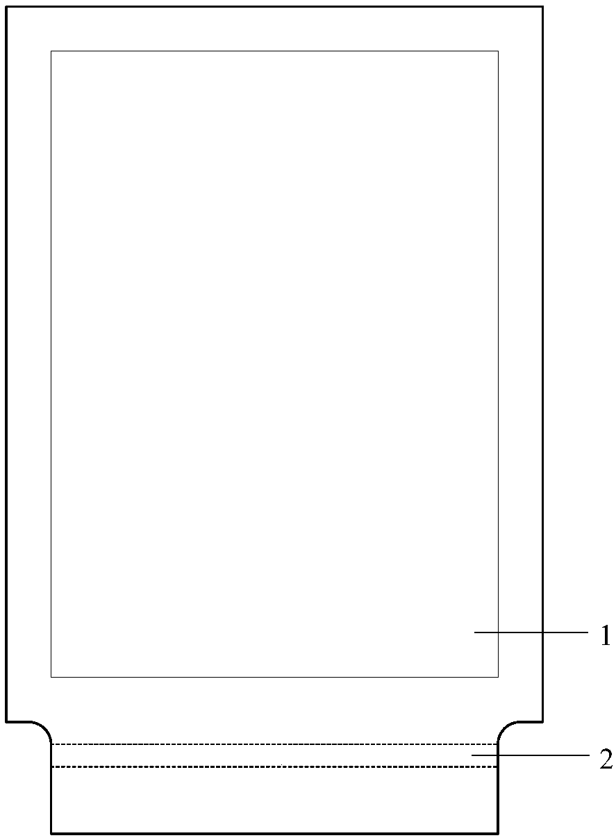
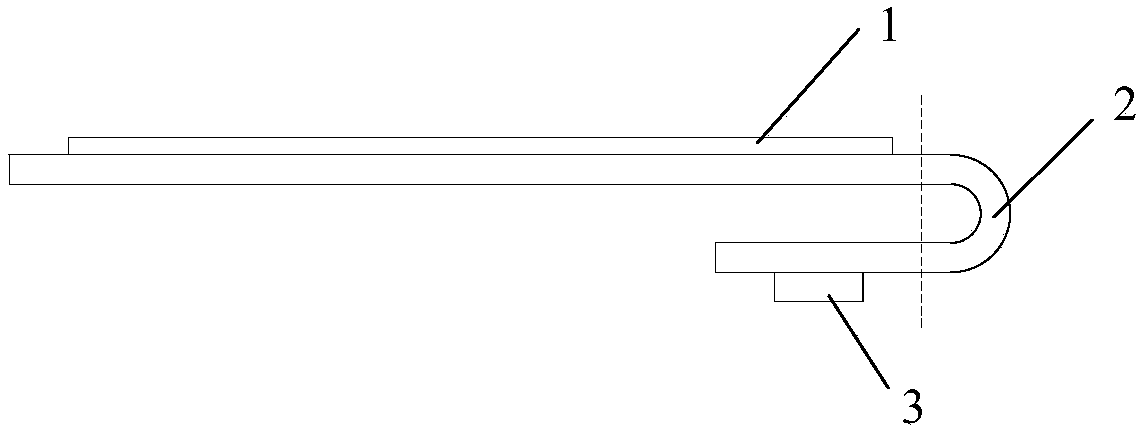
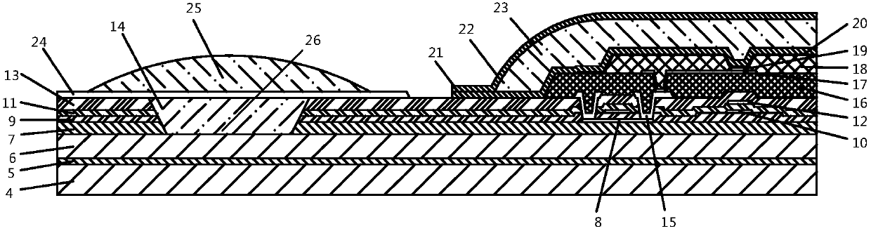
[0059] see image 3 , is a schematic structural diagram of the flexible display panel of Embodiment 1. The flexible substrate can be a three-layer structure in which an inorganic layer 5 is sandwiched between the organic layers 4 and 6 . Each thin film transistor in the sub-pixel array on the flexible substrate may include an isolation buffer layer 7, an active layer 8, a first gate insulating layer 9, a first gate layer 10, and a second gate insulating layer stacked in sequence. 11. The second gate layer 12, the dielectric layer 13, the source-drain metal layer 15 and the planar layer 16. This structure is a double-gate structure; when it is a double-gate structure, the isolation insulating layer includes The dielectric layer, the second gate insulating layer, the first gate insulating layer and the isolation buffer layer. However, in other exemplary embodiments of the present invention, each thin film transistor in the sub-pixel array may also include an isolation buffer l...

Embodiment 2

[0069] see Figure 4 , is a schematic structural diagram of the flexible display panel of the second embodiment. The grooves in this embodiment can be made by stepwise etching. In the bending area, the dielectric layer, the second gate insulating layer, the first gate insulating layer, the isolation layer, and the buffer layer extending to the non-display area can be etched in two steps. In the first step, the dielectric layer, the second gate insulating The insulating layer and the first gate insulating layer are etched to form a wider area, and the second step is to etch the isolation layer and buffer layer to form a relatively narrower area than the upper layer, forming a gentle step with a slope angle of less than 90 degrees, and the etching width It can be 1 mm to 5 mm. The etching process may be dry etching, and the dry etching gas may be CF4 / SF6 / NF3 / CH2F2 / CHF3 or the like.

[0070] The first buffer layer 14 is filled in the groove, and the thickness of the first buff...


PUM

PropertyMeasurementUnit
Slope angleaaaaaaaaaa
Thicknessaaaaaaaaaa

Abstract

The present invention provides a flexible display panel, a preparation method thereof and a flexible display device, and belongs to the technical field of flexible display. The flexible display panelprovided by the present invention comprises: a flexible substrate which includes a bending area and a display area and a non-display area on both sides of the bending area; the display area is provided with a sub-pixel array and a signal line, and the non-display area is provided with a driving chip; an isolating insulation layer which is arranged on the flexible substrate; a trench which is located in the bending area and runs through the isolating insulation layer; a first buffer layer which is filled in the trench; a lead wire which is arranged on the isolating insulation layer of the non-display area and the first buffer layer and is used for electrical connection between the driving chip and the signal line; and a second buffer layer which is located on the lead wire and at least covers the bending area. The display panel can adjust the stress neutral layer of the bending area, reduce the stress on the lead wire and improve the folding performance.

Description

technical field [0001] The invention belongs to the field of flexible display technology, and in particular relates to a flexible display panel, a method for preparing the flexible display panel, and a flexible display device. Background technique [0002] Since the OLED (Organic Light-Emitting Diode, Organic Light-Emitting Diode) display is self-luminous through the organic layer, it does not need a backlight source, nor does it need to use the optical characteristics of liquid crystals to display, so it has a faster response time and greater reliability. viewing angle, higher contrast, lighter weight, lower power consumption and other performance. OLED display is considered to be the flat panel display with the most development potential, and is considered to be the display most likely to be made into a flexible display. At present, flexible AMOLED (Active-matrix organic light emitting diode, active-matrix organic light-emitting diode) display screens have become the main...

Claims


Application Information

Patent Timeline
IPC IPC(8): H01L27/12H01L27/32
CPCH01L27/1218Y02P70/50H10K59/131H10K77/111H10K50/844H10K59/1201H10K2102/311H10K71/00
Inventor 张子予孙韬
Owner BOE TECH GRP CO LTD
Why Eureka
Try Eureka