Fabrication method of photoelectric diode and photoelectric diode

A technology of photodiodes and diodes, which is applied in the direction of circuits, electrical components, semiconductor devices, etc., can solve the problems of affecting the surface state of photodiodes, reducing the reliability of photodiodes, and contamination of photodiodes, so as to improve work stability, reduce pollution and Effects of ion damage and increased switching speed

Active Publication Date: 2019-05-14
勒威半导体技术(嘉兴)有限公司
View PDF3 Cites 0 Cited by
  • Summary
  • Abstract
  • Description
  • Claims
  • Application Information

AI Technical Summary

Problems solved by technology

[0003] At present, according to different performance parameters of photodiodes, they are applied to different fields. In the actual preparation process of photodiodes, mutual dissolution between metals and semiconductors often occurs when etching metals, resulting in contamination or damage to photodiodes. This greatly affects the surface state of the photodiode and reduces the reliability of the photodiode

Method used


Image

  • Fabrication method of photoelectric diode and photoelectric diode
  • Fabrication method of photoelectric diode and photoelectric diode
  • Fabrication method of photoelectric diode and photoelectric diode

Examples


Embodiment Construction

[0023] In order to understand the specific technical solutions, features and advantages of the present invention more clearly, the present invention will be further described in detail below with reference to the accompanying drawings and specific embodiments.

[0024] In the description of the present invention, it should be noted that the terms "upper", "lower", "left", "right", "horizontal", "longitudinal", "horizontal", "inner", "outer" and the like indicate The orientation or positional relationship is based on the orientation or positional relationship shown in the accompanying drawings, or the orientation or positional relationship that the product of the invention is usually placed in use, only for the convenience of describing the present invention and simplifying the description, rather than indicating or implied. The device or element referred to must have a particular orientation, be constructed and operate in a particular orientation, and therefore should not be co...


PUM


Abstract

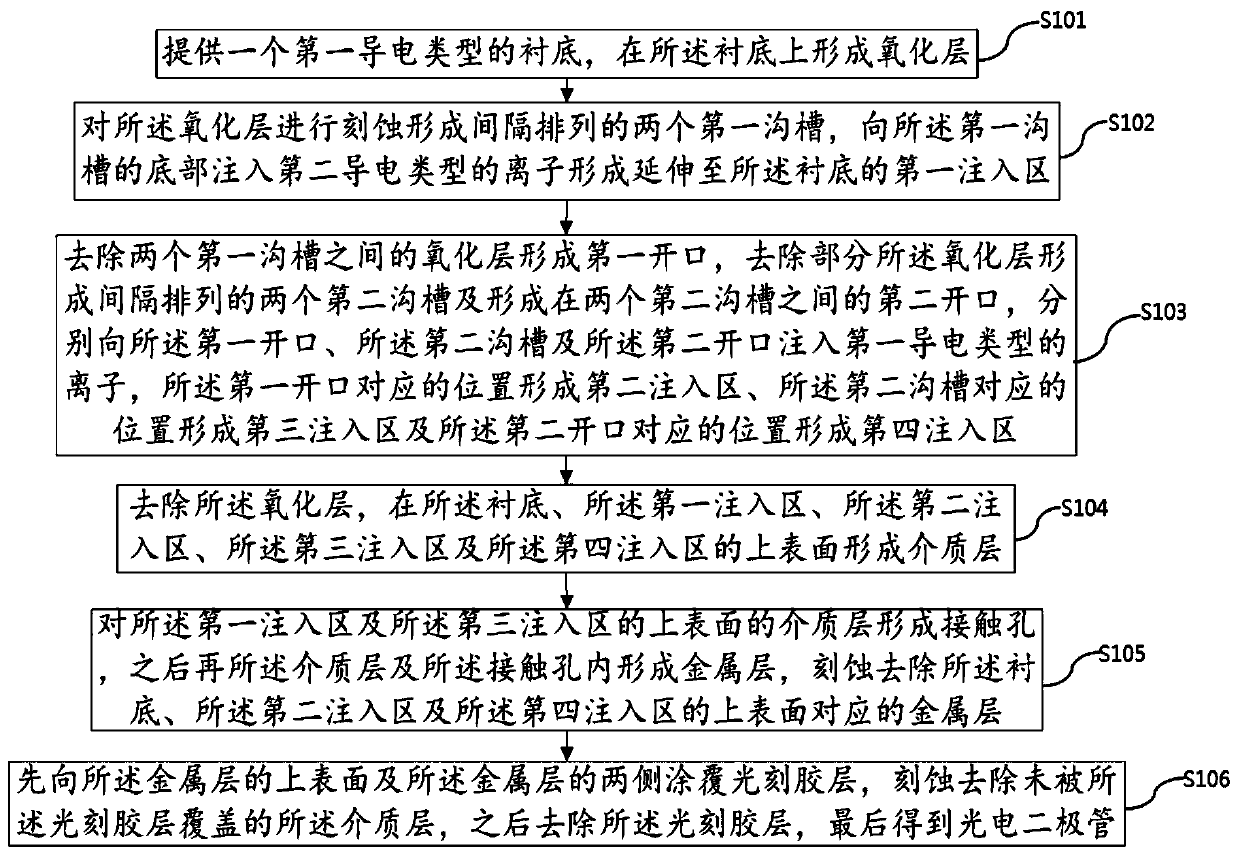
The invention provides a fabrication method of a photoelectric diode and the photoelectric diode. The fabrication method comprises the steps of S101, forming an oxide layer on a substrate; S102, forming two first grooves in the oxide layer at intervals, and forming first injection regions at the bottoms of the two first grooves; S103, forming a first opening, two second grooves and a second opening in the substrate, and injecting ions to corresponding positions to form a second injection region, a third injection region and a fourth injection region, wherein the second opening is arranged between the two second grooves; S104, removing the oxide layer, and forming dielectric layers on the substrate; S105, performing etching on the dielectric layers on the first injection region and the third injection region to form contact holes, and forming metal layers in the dielectric layers and the contact holes; and S106, coating photoresist layers on upper surfaces and two sides of the metal layers, etching and removing the dielectric layers which are not covered by the photoresist layers, removing the photoresist layers, and finally obtaining the photoelectric diode. The invention also provides the photoelectric diode, and the surface state and the reliability are improved.

Description

technical field [0001] The invention relates to the technical field of semiconductor chip manufacturing processes, in particular to a preparation method of a photodiode and a photodiode. Background technique [0002] Ordinary diodes are in a cut-off state when reverse voltage is applied, and only a weak reverse current can flow. When designing and manufacturing photodiodes, try to make the area of ​​the PN junction relatively large in order to receive incident light. The photodiode works under the action of reverse voltage. When there is no light, the reverse current is extremely weak, which is called dark current; when there is light, the reverse current rapidly increases to tens of microamps, which is called photocurrent. The greater the intensity of the light, the greater the reverse current. The change of light causes the photodiode current to change, which can convert the light signal into an electrical signal and become a photoelectric sensor device. [0003] At pres...

Claims


Application Information

Patent Timeline
Patent Type & Authority Applications(China)
IPC IPC(8): H01L31/0352H01L31/102H01L31/18
Inventor 不公告发明人
Owner 勒威半导体技术(嘉兴)有限公司
Why Eureka
Try Eureka