Method for preparing ultrathin pinhole-free dielectric films

A dielectric film and ultra-thin film technology, applied in the field of preparing ultra-thin pinhole-free dielectric films, can solve the problems of affecting the dielectric properties of the gate layer, poor uniformity of the dielectric film, and large particle size of the target material, etc. Large-area controllable thickness and uniformity, no pinhole defects, and strong adhesion

Inactive Publication Date: 2019-05-17
NANJING UNIV
View PDF4 Cites 1 Cited by
  • Summary
  • Abstract
  • Description
  • Claims
  • Application Information

AI Technical Summary

Problems solved by technology

[0005] At present, magnetron sputtering is used in the industry and scientific research circles to prepare dielectric layer films by directly sputtering dielectric insulating targets with radio frequency sources. However, due to the high energy of magnetron sputtering coatings, high-voltage sputtering The particle size of the target material is relatively large, especially when using radio frequency magnetron sputtering to coat dielectric materials, there will be problems of reverse sputtering. Therefore, the dielectric film prepared by direct magnetron sputtering usually has poor uniformity and insufficient density. , and there are many pinholes, which seriously affect the dielectric properties of the gate layer, leading to problems such as low yield of the device

Method used


Image

  • Method for preparing ultrathin pinhole-free dielectric films
  • Method for preparing ultrathin pinhole-free dielectric films
  • Method for preparing ultrathin pinhole-free dielectric films

Examples


specific Embodiment

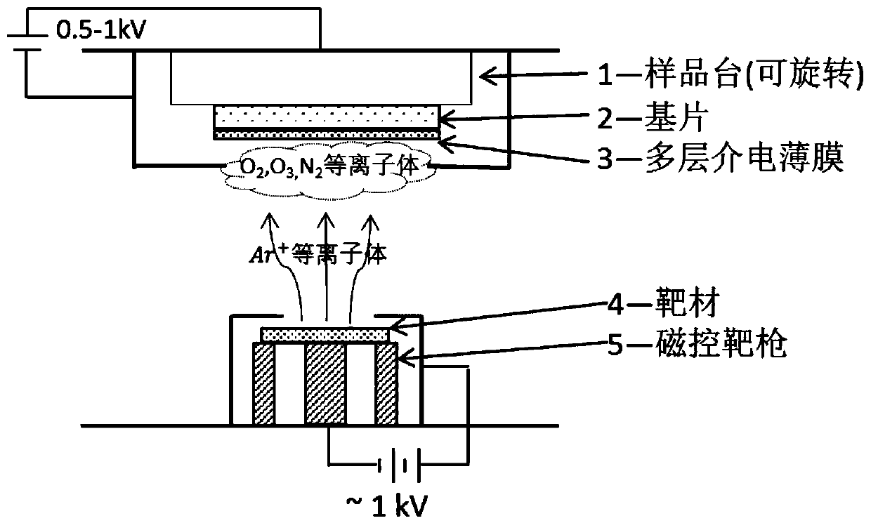
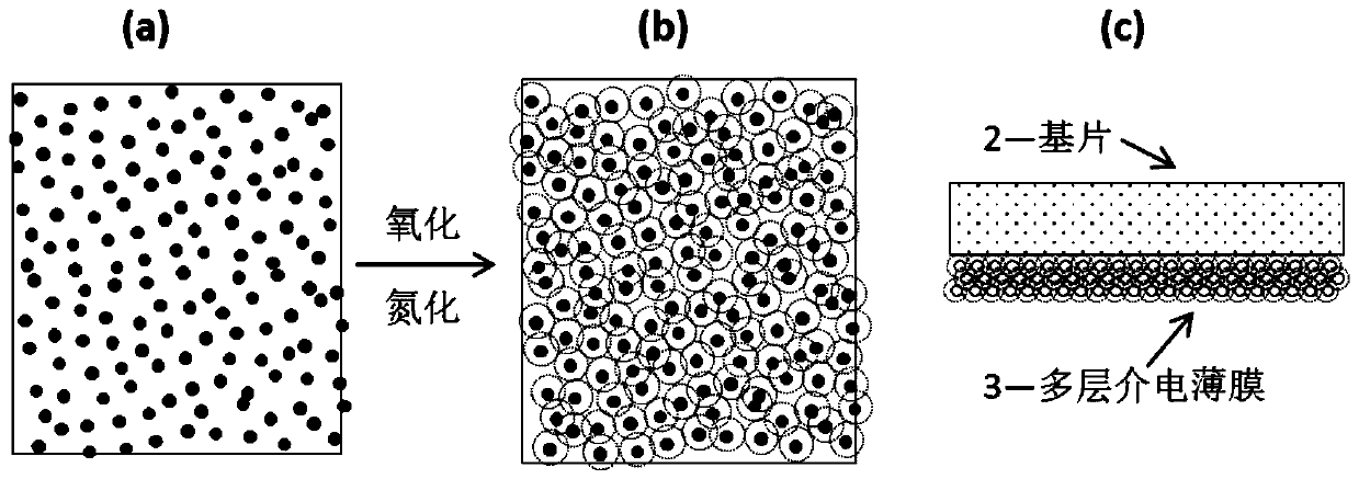
[0035] The metal oxide dielectric film Ta 2 o 5 Take as an example to illustrate the specific operation and preparation process.

[0036] The magnetron sputtering apparatus used in this embodiment is divided into a main cavity for film growth and an attached cavity for pre-stage sample introduction, Si / SiO 2 (300nm) substrates are delivered to the main chamber of magnetron sputtering through the front-stage sample feeding chamber. The first step is to deposit metal tantalum film: the vacuum degree on the back of the main cavity reaches 2*10 -8 After the Torr is below, open the gas flow meter and feed pure Ar gas into the magnetron sputtering apparatus to stabilize the air pressure in the main chamber at 3.8*10 -3 torr; turn on the DC magnetron sputtering power supply and set the output power to 25 watts, and the deposition rate of tantalum detected by the film thickness detector is 0.023nm / s; ) the substrate is rotated directly above the tantalum target for deposition and ...


PUM

PropertyMeasurementUnit
thicknessaaaaaaaaaa

Abstract

The invention discloses a method for preparing ultrathin pinhole-free dielectric films. The method comprises the steps that (1), 0.5-1nm ultrathin films are obtained by deposition through a physical vapor deposition method; (2), the 0.5-1nm ultrathin metal films or ultrathin nonmetal films obtained in the step (2) are subjected to a redox reaction through gas plasma with oxidation characteristics;and (3), the step (1) and the step (2) are repeatedly carried out according to the target thickness of the to-be-prepared ultrathin pinhole-free dielectric films, and the ultrathin pinhole-free dielectric films with the target thickness are obtained. The method for preparing the ultrathin pinhole-free dielectric films has no chemical corrosion, can be in situ in the same cavity, and is high in film forming speed; and the ultrathin pinhole-free dielectric films prepared by the method has high adhesivity, high compactness and no pinhole defect, and the thickness and the uniformity can be controlled in a large area.

Description

technical field [0001] The invention relates to a method for preparing various dielectric films in the fields of traditional microelectronics and novel spin electronics, in particular to a method for preparing a pinhole-free dielectric film based on a physical vapor deposition method. Background technique [0002] At present, there are mainly two methods of film preparation: chemical vapor deposition and physical vapor deposition. Chemical vapor deposition is a chemical technology. A method in which a chemical reaction occurs on a surface to form a thin film. Physical Vapor Deposition (Physical Vapor Deposition, PVD) technology uses physical methods to vaporize material sources into gaseous atoms, molecules or parts into ions under vacuum conditions, and through a low-pressure gas (or plasma) process, on the surface of the substrate The technology of depositing thin films with certain special functions. [0003] There are problems such as the limit of oxidation reaction an...

Claims


Application Information

Patent Timeline
Patent Type & Authority Applications(China)
IPC IPC(8): C23C14/06C23C14/08C23C14/14C23C14/22C23C14/35C23C14/58
Inventor 陈丽娜刘荣华李丽媛都有为
Owner NANJING UNIV
Why Eureka
Try Eureka