LED epitaxial layer with new-type PSS structure and preparation method thereof

An epitaxial layer, a new type of technology, applied in electrical components, circuits, semiconductor devices, etc., can solve the problems of high dislocation density of GaN materials, improved product quality, lattice mismatch, etc., to improve the light extraction efficiency and increase the light extraction angle. , The effect of simple process route

Inactive Publication Date: 2019-05-21
XIANGNENG HUALEI OPTOELECTRONICS
View PDF5 Cites 4 Cited by
  • Summary
  • Abstract
  • Description
  • Claims
  • Application Information

AI Technical Summary

Problems solved by technology

At present, the industry mainly adopts MOCVD (metal organic compound chemical vapor deposition) method to prepare LED epitaxial wafers. Due to factors such as errors and lattice mismatches in the production process, the prepared GaN material has high dislocation density, Defects such as difficulty in improving product quality

Method used


Image

  • LED epitaxial layer with new-type PSS structure and preparation method thereof
  • LED epitaxial layer with new-type PSS structure and preparation method thereof
  • LED epitaxial layer with new-type PSS structure and preparation method thereof

Examples


Embodiment 1

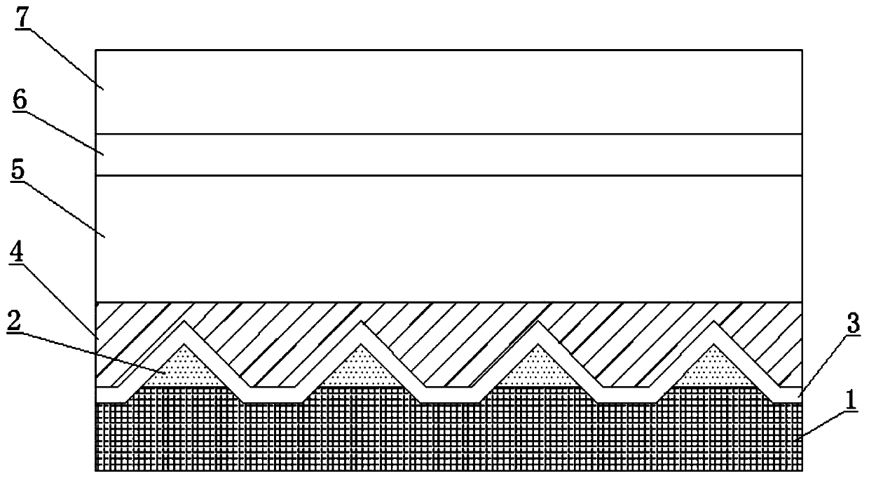
[0029] see Figure 1 ~ Figure 4 , a LED epitaxial layer with a new PSS structure, including a patterned substrate arranged in sequence along the axial direction, a U-type GaN layer 4 without Si doping, an N-type GaN layer 5 doped with Si, and an MQW active layer 6 and a p-type GaN layer 7 .

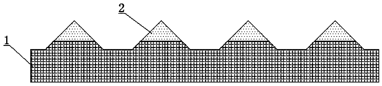
[0030] The patterned substrate includes a substrate material 1 and a substrate pattern arranged on the substrate material 1, the substrate pattern is a cone uniformly arranged in an array, and the cone includes a PSS film arranged up and down Projection structure of layer 2 and substrate material 1.

[0031] In this embodiment, the material of the substrate material 1 is sapphire, and the material of the PSS film layer 2 is silicon oxide.

[0032] In this embodiment, a layer of aluminum nitride film 3 is further provided between the patterned substrate and the U-shaped GaN layer 4, and the thickness of the aluminum nitride film 3 is 20 nm.

[0033] The preparation method of the LED epi...


PUM


Abstract

The invention provides an LED epitaxial layer with a new-type PSS structure. The LED epitaxial layer comprises a patterned sapphire substrate, a U type GaN layer, an N type GaN layer, an MQW active layer and a P type GaN layer which are set in sequence. The patterned sapphire substrate comprises a substrate material and substrate patterns which are arranged on the substrate material according to an array. The substrate patterns are cones. Bottom diameters of the cones are 1.5-3.5um. Heights of the cones are 0.8-2.5um. Each cone comprises a PSS film layer and a substrate material convex structure which are set up and down or only comprises the PSS film layer. A material of the PSS film layer is combined by one or more of silicon oxide, silicon nitride, aluminium nitride and silicon oxynitride. An aluminium nitride film layer is also set between the patterned sapphire substrate and the U type GaN layer. The invention also provides a preparation method for the LED epitaxial layer. According to the LED epitaxial layer and the preparation method, through setting of a PSS substrate of a composite material, total reflection of light is improved and light extraction efficiency of a chip iseffectively improved.

Description

technical field [0001] The invention relates to the technical field of LED semiconductor production, in particular to an LED epitaxial layer with a novel PSS structure and a method for preparing the LED epitaxial layer. Background technique [0002] LED products are widely used in all walks of life and play an important role in people's daily life and production. At present, the industry mainly adopts MOCVD (metal organic compound chemical vapor deposition) method to prepare LED epitaxial wafers. Due to factors such as errors and lattice mismatches in the production process, the prepared GaN material has high dislocation density, Defects such as difficulty in improving product quality. Therefore, how to prepare more perfect epitaxial wafers is the direction of efforts in the process of industrial mass production of LED products. [0003] Patterned Sapphire Substrate (PSS), that is, a mask for dry etching is grown on the substrate material, and the mask is etched into a pat...

Claims


Application Information

Patent Timeline
Patent Type & Authority Applications(China)
IPC IPC(8): H01L33/10H01L33/22H01L33/00
Inventor 周智斌谈健汪延明
Owner XIANGNENG HUALEI OPTOELECTRONICS
Why Eureka
Try Eureka