Full-inorganic LED packaging structure and preparation method thereof

A technology of LED packaging and LED chips, which is applied in the direction of semiconductor devices, electrical components, circuits, etc., can solve the problems of easy ventilation and low reliability of LED devices, and achieve the effects of stable chemical properties, good adhesion effect, and low price

Inactive Publication Date: 2019-05-21
EZHOU INST OF IND TECH HUAZHONG UNIV OF SCI & TECH +1
View PDF7 Cites 7 Cited by
  • Summary
  • Abstract
  • Description
  • Claims
  • Application Information

AI Technical Summary

Problems solved by technology

[0004] Aiming at the above defects or improvement needs of the prior art, the present invention provides an all-inorganic LED packaging structure and packaging method, the purpose of which is to solve the problem of low reliability of the LED device obtained by the LED packaging technology in the prior art and easy air permeability and moisture permeability. technical issues

Method used


Image

  • Full-inorganic LED packaging structure and preparation method thereof
  • Full-inorganic LED packaging structure and preparation method thereof
  • Full-inorganic LED packaging structure and preparation method thereof

Examples


preparation example Construction

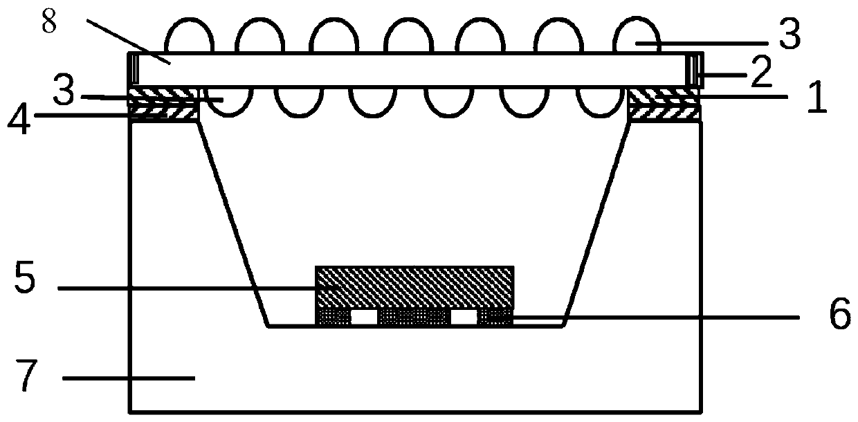
[0045] The present invention also provides a method for preparing the above-mentioned all-inorganic LED packaging structure, which includes the following steps:

[0046] LED chip bonding: bonding the LED chip 5 inside the dam-type copper-clad ceramic substrate 7;

[0047] Preparation of the first metal layer: the first metal layer 1 is vapor-deposited on the area where the lower surface of the flat quartz glass 8 is in contact with the copper-clad ceramic substrate 7 by electron beam evaporation.

[0048] Complete the LED packaging: cover the flat quartz glass 8 with the first metal layer 1 on the copper-clad ceramic substrate 7 and put it into the reflow furnace for soldering and bonding.

[0049] The preparation method of the all-inorganic LED packaging structure of the present invention is simple and ensures the reliability of LED device packaging. And it is worth mentioning that the quartz glass metallization involved in the present invention can not only be used for deep ultravio...

Embodiment 1

[0059] LED chip solid crystal:

[0060] The LED chip 5 is passed through the second bonding layer 6 (solder paste) in a reflow furnace through five temperature zones to reflow and change, the highest temperature is 270 ℃, so that the chip and the copper-clad ceramic substrate 7 electrothermal separation area form a good bond, thereby The LED chip 5 is packaged inside a dam-type copper-clad ceramic substrate 7.

[0061] Prepare the first metal layer:

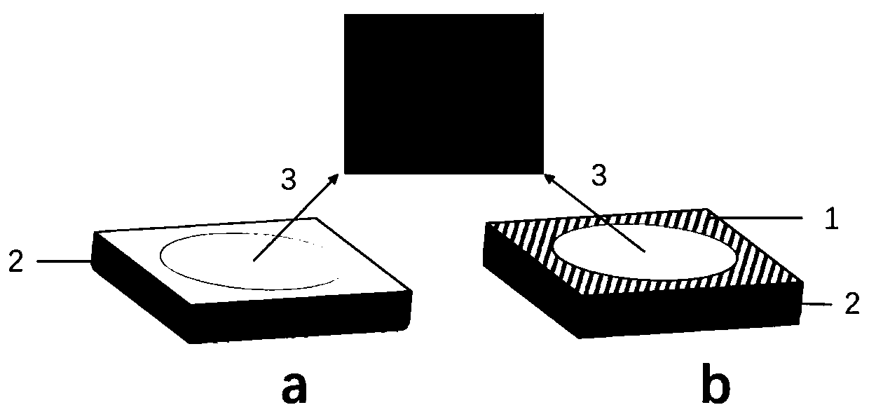
[0062] First, the corresponding metal light window layout is prepared according to the size of the copper-clad ceramic substrate 7. The size of the metal light window is 3.6mm×3.6mm, and the diameter of the middle circle is 3.04mm. The size of a metal layer 1 is the area excluding the circle, and this area is the pattern of the metal light window.

[0063] 1. Make the first metal layer on the flat quartz glass.

[0064] 1.1 Cleaning the sample: soak a 2-inch flat quartz glass 8 in ultrasonically heated acetone for 5 minutes to remove org...

Embodiment 2

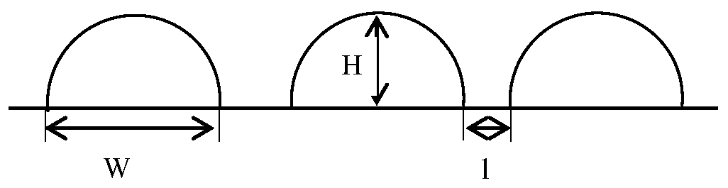
[0087] Embodiment 2 (a nano-microlens array is set on the upper surface)

[0088] Compared with embodiment 1, the difference of this embodiment 2 is that this embodiment only prepares the nano-microlens array on the upper surface of the flat quartz glass, and the other preparation methods are the same.


PUM

PropertyMeasurementUnit
thicknessaaaaaaaaaa
widthaaaaaaaaaa
heightaaaaaaaaaa

Abstract

The invention belongs to the field of LED devices, and discloses a full-inorganic LED packaging structure. The full-inorganic LED packaging structure comprises a box dam type copper coated ceramic substrate, an LED chip in the copper coated ceramic substrate, plane quartz glass at the top of the copper coated ceramic substrate and a first metal layer on the lower surface of the plane quartz glass,wherein the first metal layer has a size equal to the size of a contact area between the plane quartz glass and the copper coated ceramic substrate; the first metal layer comprises Cr, Pt and Au metal layers in sequence from top to bottom; and the total thickness of the first metal layer is 0.9-2 microns. The invention furthermore discloses a preparation method of the full-inorganic LED packagingstructure, and the preparation method comprises the steps of carrying out solid phase crystallization on the LED chip, preparing the first metal layer and completing LED packaging. The invention aimsat solving the technical problem that the LED devices obtained through LED packaging technologies in the prior art are low in reliability and easy to permeate air and moisture.

Description

Technical field [0001] The invention belongs to the field of LED devices, and more specifically, relates to an all-inorganic LED packaging structure and a preparation method thereof. Background technique [0002] For optical devices, its light extraction efficiency and reliability are important parameters to measure device performance. For example, in LED packaging, in order to protect the chip, most of them still use a layer of organic packaging materials such as silica gel and epoxy resin on the chip surface. Although this packaging process does not require additional development of new equipment and materials, the process is relatively mature, and the cost is relatively low, but under long-term high temperature and high-energy radiation, organic polymer materials will undergo molecular dissociation and destruction, and organic packaging materials will be damaged. The quality and hardness will be affected, and the phenomenon of aging and yellowing will occur, which greatly red...

Claims


Application Information

Patent Timeline
Patent Type & Authority Applications(China)
IPC IPC(8): H01L33/48H01L33/54H01L33/56H01L33/58
Inventor 许琳琳张爽梁仁瓅龙瀚凌王昊陈长清戴江南
Owner EZHOU INST OF IND TECH HUAZHONG UNIV OF SCI & TECH
Why Eureka
Try Eureka