High-range acceleration sensor ceramic silicon ceramic three-layer leadless package structure

A technology of acceleration sensor and packaging structure, which is applied in the direction of measuring acceleration, speed/acceleration/shock measurement, measuring device, etc. It can solve the problems of increasing the volume and reducing the reliability of the sensor, so as to reduce the volume, realize leadless packaging, The effect of reducing noise

Active Publication Date: 2021-04-02
ZHONGBEI UNIV
View PDF20 Cites 0 Cited by
  • Summary
  • Abstract
  • Description
  • Claims
  • Application Information

AI Technical Summary

Problems solved by technology

Due to the existence of gold wire bonding and PCB board, the volume of the package is increased, and the reliability of the sensor under high impact conditions is greatly reduced.

Method used


Image

  • High-range acceleration sensor ceramic silicon ceramic three-layer leadless package structure
  • High-range acceleration sensor ceramic silicon ceramic three-layer leadless package structure
  • High-range acceleration sensor ceramic silicon ceramic three-layer leadless package structure

Examples


Embodiment 1

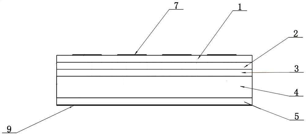
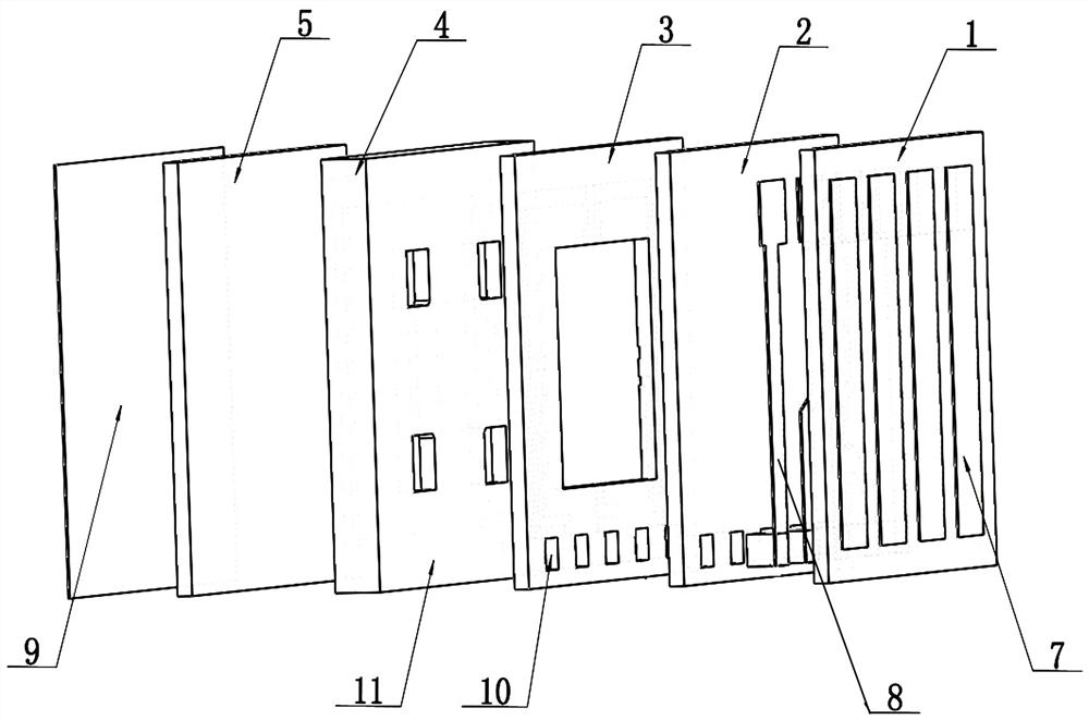
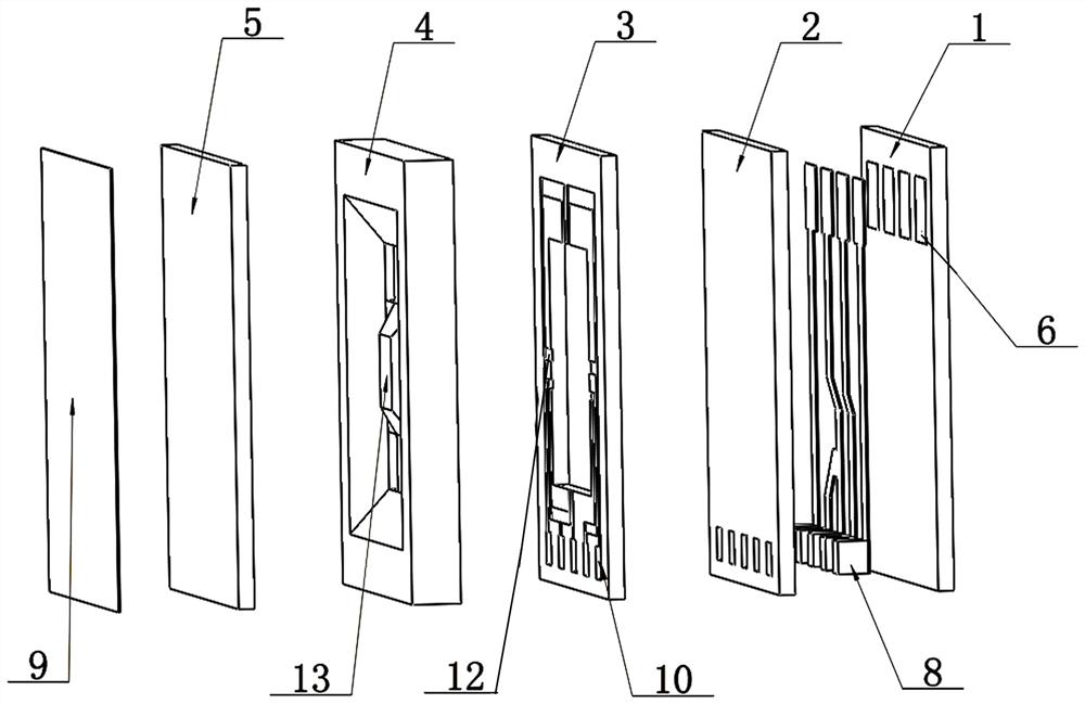
[0021] Such as Figure 1-Figure 3 As shown, a high-range acceleration sensor ceramic silicon ceramic three-layer leadless packaging structure includes a bottom layer of cooked ceramic chip 5, a sensitive structure 4, a third layer of cooked ceramic chip 1, a second layer of cooked ceramic chip 2, a first layer of cooked ceramic chip Ceramic sheet 3, the bottom surface of the bottom cooked porcelain sheet 5 is brushed with brazing paste 9, and the top surface of the bottom cooked porcelain sheet 5 is bonded to the back of the sensitive structure 4 using anodic bonding technology. The front side of the sensitive structure 4 is also bonded to the three-layer cooked porcelain sheet by anodic bonding technology, and the three-layer cooked porcelain sheet is respectively the first layer of cooked porcelain sheet 3 and the second layer of cooked porcelain sheet arranged from bottom to top. Sheet 2 and the third layer of cooked porcelain sheet 1, wherein the first layer of cooked porc...


PUM


Abstract

The invention relates to a sensor chip packaging structure, in particular to a ceramic silicon ceramic three-layer leadless packaging structure of a high-range acceleration sensor, which comprises a layer of low-temperature co-fired ceramic sheets with one surface capable of being grounded and brazed, wherein the non-brazed surface adopts an anode bonding technology to achieve bonding of a cookedceramic sheet and the back surface of a sensitive structure; the front surface of the sensitive structure is also bonded with the three layers of cooked ceramic sheets by adopting the anode bonding; the first layer is a low-temperature co-fired ceramic frame with the same area as a sensor frame, meanwhile, PAD points of the sensitive structure are connected to the second layer circuit through laser perforating and filling holes by using slurry, the second layer achieves the function of circuit transfer through slurry printing, and transmits signals to the third layer of the cooked ceramic sheets, namely the top layer of the packaging structure; the top layer of the packaging structure is coated with brazing slurry, therefore, the cooked ceramic sheet can be connected with output wires through brazing. According to the invention, the packaging structure area is minimized, the leadless packaging of the acceleration sensor is achieved, and the reliability of the sensor is greatly improved.

Description

technical field [0001] The invention relates to a sensor chip packaging structure, in particular to a three-layer non-lead packaging structure of ceramic silicon ceramics for a high-range acceleration sensor. Background technique [0002] Low-temperature co-fired ceramic (LTCC) technology is a low-cost packaging technology. The ceramic material has excellent high-frequency and high-quality factor characteristics. Using low-temperature co-fired ceramics to achieve circuit transfer has better thermal conductivity than ordinary PCB circuit substrates. , better temperature characteristics. Due to the small thermal expansion coefficient and dielectric constant temperature coefficient of low-temperature co-fired ceramics, the residual stress generated during the anodic bonding process with silicon chips is small. The existing high-range acceleration sensor packages all use gold wire bonding to connect the sensitive structure with the PCB adapter board, and then the output wires a...

Claims


Application Information

Patent Timeline
Patent Type & Authority Patents(China)
IPC IPC(8): G01P15/00
Inventor 石云波刘俊唐军曹慧亮焦静静郭涛高晋阳李杰张晓明马宗敏赵永祺赵思晗许鑫李飞王彦林张英杰米振国张婕刘玉
Owner ZHONGBEI UNIV
Why Eureka
Try Eureka