Organic electroluminescent device containing capping layer and application thereof

An electroluminescence device and luminescence technology, applied in the direction of circuits, electrical components, electric solid devices, etc., can solve the problems of reducing the angular dependence of the device and low light extraction efficiency

Active Publication Date: 2019-06-07
JIANGSU SUNERA TECH CO LTD
View PDF9 Cites 17 Cited by
  • Summary
  • Abstract
  • Description
  • Claims
  • Application Information

AI Technical Summary

Problems solved by technology

[0005] Therefore, in view of the current low light extraction efficiency of OLED devices, it is desirable to use a cover layer (light extraction material layer) that can achieve higher light extraction efficiency in the device structure, and to reduce the angular dependence of the device.

Method used


Image

  • Organic electroluminescent device containing capping layer and application thereof
  • Organic electroluminescent device containing capping layer and application thereof
  • Organic electroluminescent device containing capping layer and application thereof

Examples


Embodiment 1

[0135] Prepare an organic electroluminescent device with the following preparation steps, comprising:

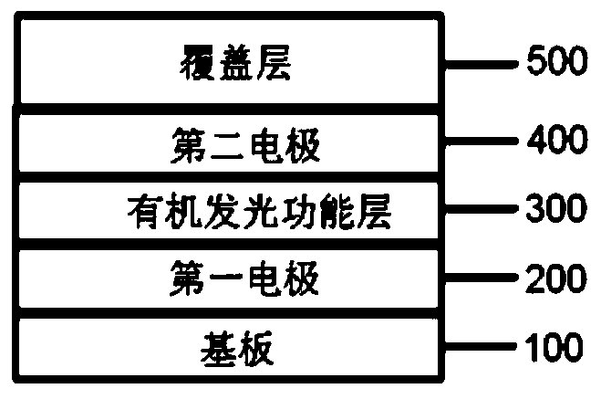
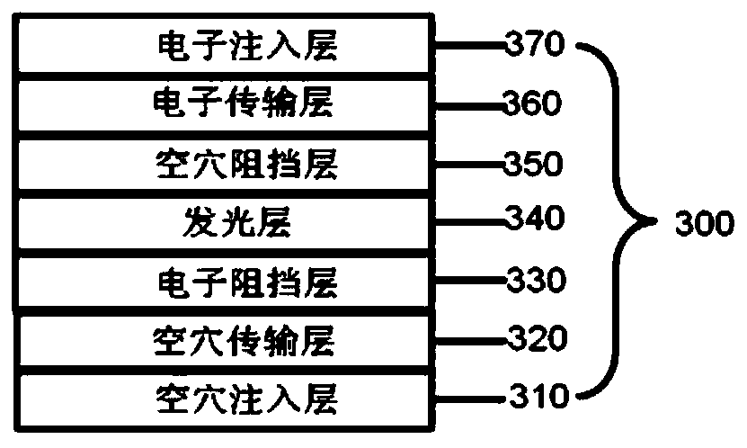
[0136] On the low-temperature polysilicon (LTPS) substrate (substrate layer 100), a 10nm ITO film (first electrode layer 200) was formed by sputtering, etched into required patterns, and ultrasonically cleaned with deionized water, acetone, and ethanol, respectively. 15 minutes, and then processed in a plasma cleaner for 2 minutes; here the ITO electrode layer is an anode, and on the ITO anode layer, the hole injection layer material HAT-CN is evaporated by vacuum evaporation, and the thickness is 10nm. As the hole injection layer 310; on the hole injection layer 310, the hole transport material NPB is evaporated by vacuum evaporation, with a thickness of 110nm, and this layer is the hole transport layer 320, which can also be used as a microcavity adjustment layer; On the hole transport layer 320, the electron blocking material TCTA is evaporated by vacuum evaporation with ...

Embodiment 2

[0138] The preparation method is the same as device embodiment 1, but adopts the following device structure:

[0139] ITO(10nm) / NPB:Compound A(97:3 mass ratio, 97 mass% NPB)(10nm) / NPB(150nm) / TCTA(10nm) / CBP:Ir(PPy) 3 (90:10 mass ratio, 90 mass% of CBP) (40nm) / / TPBI (35nm) / compound D (1nm) / Yb (1nm) / Mg:Ag (10:90 mass ratio, 10 mass% of Mg) (14 nm) / Compound 1 of the present invention (50 nm).

Embodiment 3

[0141] The preparation method is the same as device embodiment 1, but adopts the following device structure:

[0142] ITO (10nm) / NPB: Compound C (95:5 mass ratio, 95% by mass of NPB) (10nm) / NPB (190nm) / TCTA (10nm) / CBP:Ir(pq)2acac (96:4 mass ratio, 96% by mass of CBP) (40nm) / TPBI (35nm) / compound D (1nm) / Yb (1nm) / Mg:Ag (10:90 mass ratio, 10% by mass of Mg) (14nm) / Compound 1 of the present invention (50nm).

[0143] Device Embodiments 4, 7, 10, 13, 16, 19, 22, 25, 28, 31, 34, 37, 40, 43, 46, 49, 52, 55, 58, 61, 64, 67, 70, 73 , 76, 79, 82, 85, 88, 91, 94, 97, 100, 103, 106, 109, 112, 115, 118, 121, 124, 127:

[0144] The preparation method is the same as that of Device Example 1, except that compounds 6, 14, 24, 37, 42, 52, 60, 81, 91, 102, 114, 127, 137, 147, 156, 162, 174, 183,193,206,219,228,246,255,270,275,289,300,311,316,328,340,351,360,370,387,397,404,416,426,436,440 as Cover layer materials for organic electroluminescent devices.


PUM


Abstract

The invention relates to an organic electroluminescent device containing a capping layer. The organic electroluminescent device containing the capping layer comprises a substrate layer, a first electrode, an organic light emitting functional layer, a second electrode and the capping layer, wherein the first electrode is located on the substrate; the organic light emitting functional layer is located on the first electrode; the second electrode is located on the organic light emitting functional layer; and the capping layer is located on the second electrode, the capping layer comprises an organic compound, the organic compound of the capping layer contains different types of heteroarylamines and has higher glass transition temperature and molecular thermal stability. Low absorption and high refractive index in the visible light field are achieved, and the light extraction efficiency of an OLED device can be effectively improved after the organic electroluminescent device is applied toa CPL layer of an organic light Emission diode (OLED) device. The invention further relates to the application of the organic electroluminescent device containing the capping layer for display or lighting equipment.

Description

technical field [0001] The present invention relates to an organic electroluminescent device, in particular to an organic electroluminescent device which contains a capping layer and can effectively improve light extraction efficiency. Background technique [0002] Organic electroluminescent (OLED: Organic Light Emission Diodes) device technology can be used not only to manufacture new display products, but also to prepare new lighting products. It is expected to replace the existing liquid crystal display and fluorescent lighting, and has a wide application prospect. The OLED device has a sandwich structure, including electrode layers and organic light-emitting functional layers sandwiched between different electrode layers. Various electrode layers, organic light-emitting functional layers, and other related material layers are stacked together according to the application. OLED devices. The OLED device is a current-driven device. When a voltage is applied to the electrod...

Claims


Application Information

Patent Timeline
Patent Type & Authority Applications(China)
IPC IPC(8): H01L51/52H01L51/54
Inventor 陈海峰张兆超李崇唐丹丹
Owner JIANGSU SUNERA TECH CO LTD
Why Eureka
Try Eureka