Supercharge Your Innovation With Domain-Expert AI Agents!

Image sensor with compact design layout

A technology of image sensor and compact design, applied in the field of image sensor, can solve the problems of reducing the sensitivity of pixel circuit, limiting the conversion gain of pixel circuit, affecting the performance of the image sensor, etc., to save the power wiring design, improve the conversion gain, and improve the performance.

Pending Publication Date: 2019-06-14
思特威(上海)电子科技股份有限公司
View PDF0 Cites 0 Cited by
  • Summary
  • Abstract
  • Description
  • Claims
  • Application Information

AI Technical Summary

Problems solved by technology

When the parasitic capacitance of the floating diffusion point in the pixel circuit is large, the conversion gain of the pixel circuit will be limited, and the sensitivity of the pixel circuit will be reduced, thereby affecting the performance of the image sensor

Method used


Image

  • Image sensor with compact design layout
  • Image sensor with compact design layout
  • Image sensor with compact design layout

Examples


Embodiment Construction

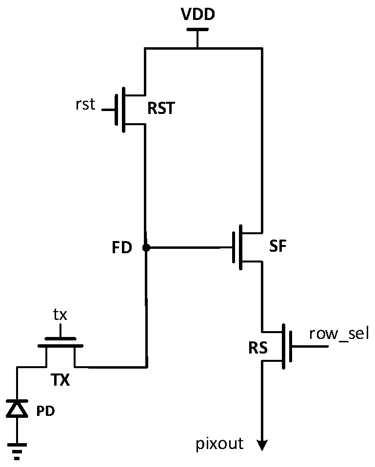
[0021] The content of the invention proposed by the patent of the present invention will be described in detail below in conjunction with each accompanying drawing. figure 1 It is the image sensor pixel circuit diagram of the basic 4T structure, such as figure 1 As shown in , the image sensor pixel circuit includes a photodiode PD and a transfer transistor TX connected to the photodiode PD, which transfers electrons accumulated in the photodiode PD during exposure to a floating diffusion FD according to a control signal tx. The reset crystal RST and the drain of the source follower transistor SF are connected to the same fixed power supply VDD. The pixel circuit further includes a row selection transistor RS, which controls and outputs the pixel signal (pixout) amplified by the source follower transistor SF to the corresponding column line according to the row selection control signal row_sel.

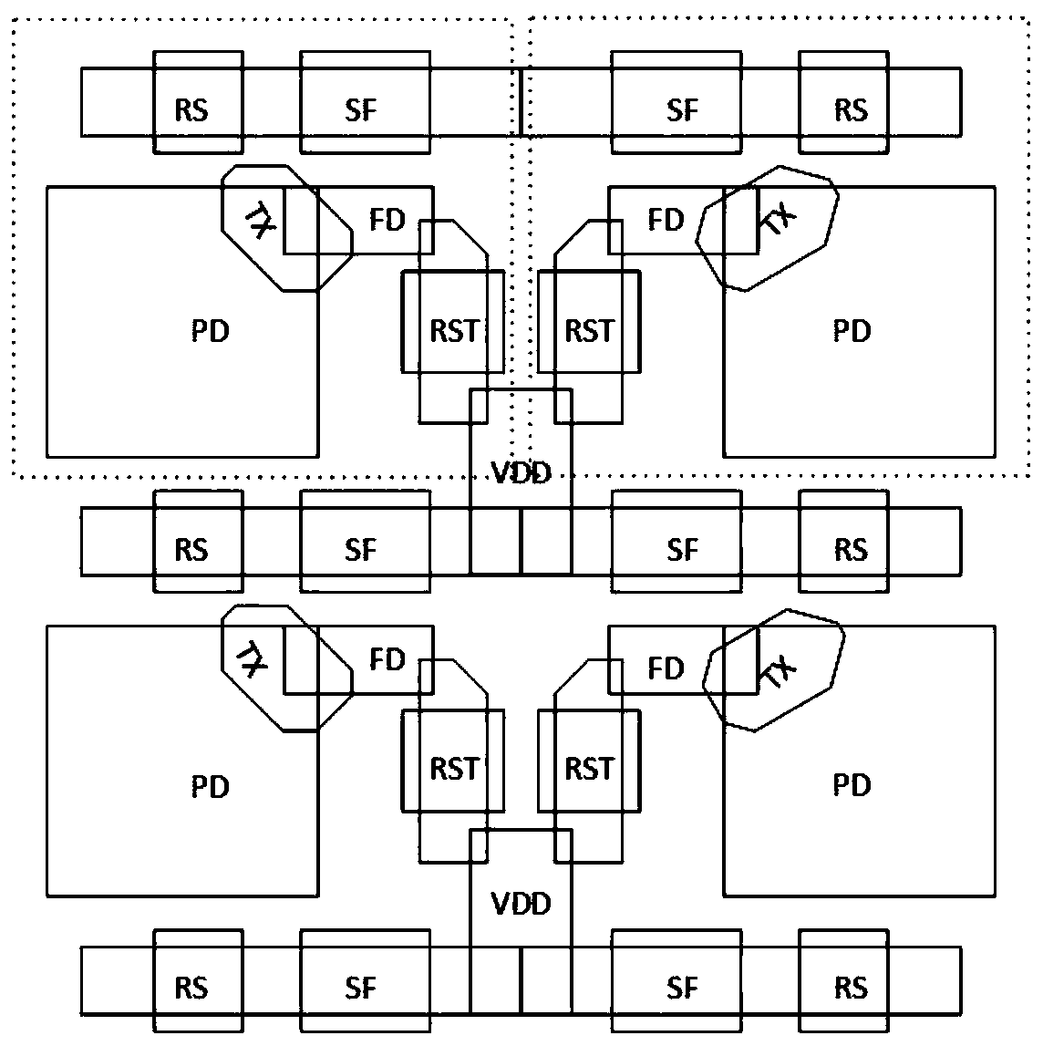
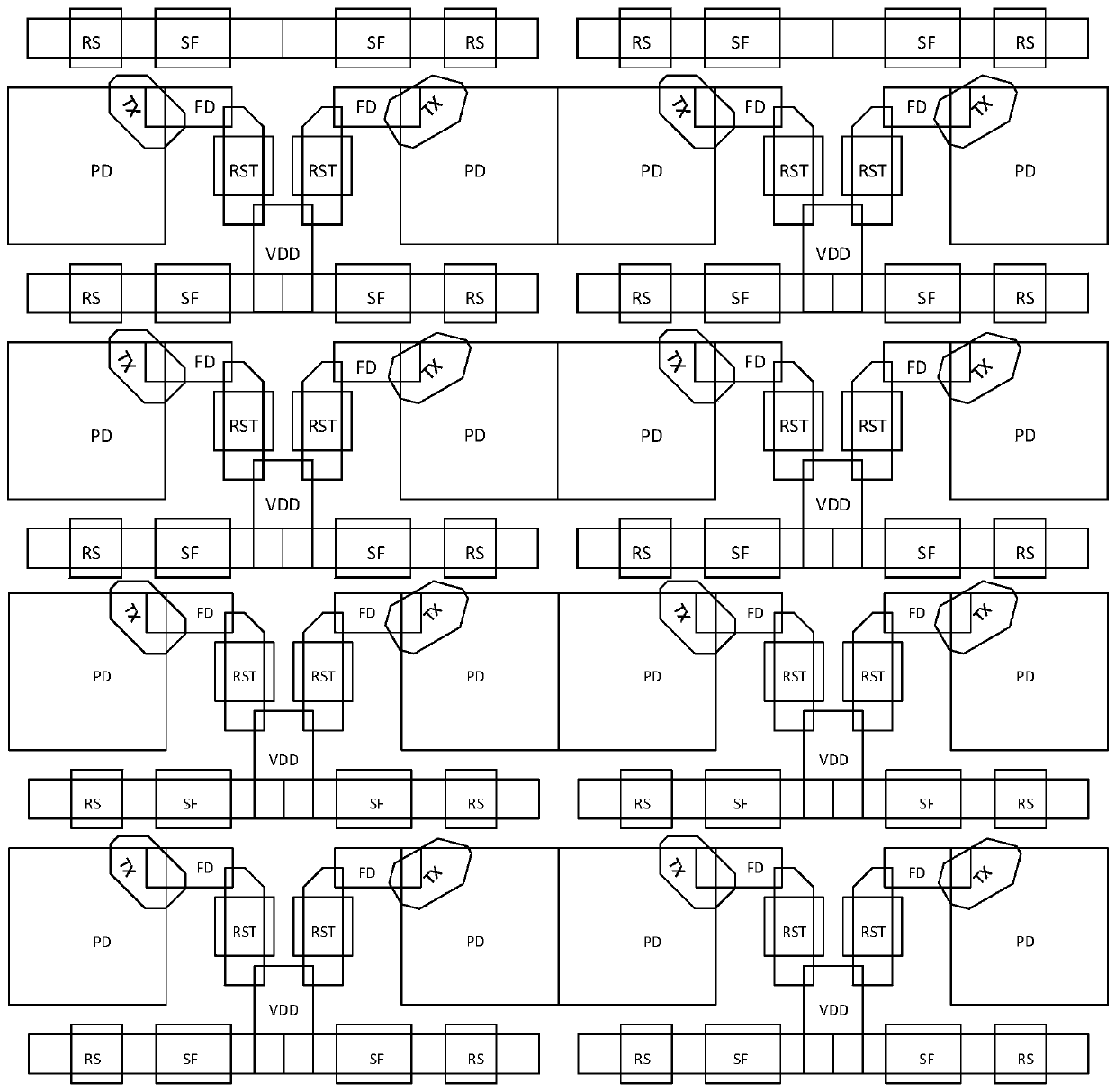
[0022] The image sensor with a compact design layout proposed by the patent of th...


PUM


Abstract

The invention provides an image sensor with compact design layout. The image sensor comprises a pixel array arranged in rows and columns on a semiconductor substrate, in the same row of the pixel array, and the pixel units in the two neighboring columns are arranged along a central line of the column direction in mirror symmetry. In each pixel unit, a photoelectric diode is distributed and arranged in one direction, a transmission transistor is arranged aslant at a corner part of the photoelectric diode according to a certain angle; a reset transistor is arranged at an edge side of the photoelectric diode; a source electrode is arranged at the edge side, neighboring to the reset transistor, of the photoelectric diode, and is close to a floating dispersion point. Two reset transistors arranged in the pixel units of two neighboring columns of the same line of the pixel array and drain electrodes of two source electrode following transistors arranged adjacently in the next neighboring line are connected to the same fixed power supply. The compact design layout structure provided by the invention can further improve performance of the image sensor.

Description

technical field [0001] The invention relates to the technical field of image sensors, in particular to an image sensor with a compact layout design and effectively improved pixel circuit performance. Background technique [0002] Image sensors are widely used in various fields, such as smartphones, surveillance equipment, drones, artificial intelligence, etc., and their application requirements are increasingly miniaturized. With the development of technology, the size of the image sensor pixel unit is further reduced, increasing the conversion gain of the pixel circuit and improving the sensitivity of the image sensor is the direction of its development and improvement. In the design of the image sensor, adopting a reasonable layout design structure can effectively improve the performance of the image sensor. For example, the layout structure is compact, and the arrangement structure of each device in the pixel unit is reasonable, which reduces the impact on the photosensi...

Claims


Application Information

Patent Timeline
Patent Type & Authority Applications(China)
IPC IPC(8): H01L27/146
Inventor 王欣徐辰
Owner 思特威(上海)电子科技股份有限公司
Features
  • R&D
  • Intellectual Property
  • Life Sciences
  • Materials
  • Tech Scout
  • Unparalleled Data Quality
  • Higher Quality Content
  • 60% Fewer Hallucinations
Learn More