AlN template, light-emitting diode epitaxial wafer and production method thereof

A technology for light-emitting diodes and manufacturing methods, applied in electrical components, circuits, semiconductor devices, etc., can solve the problems of poor wavelength uniformity of epitaxial wafers, lattice mismatch, etc., to improve wavelength uniformity, increase lattice constant, The effect of preventing the deterioration of crystal quality

Inactive Publication Date: 2019-06-14
HC SEMITEK ZHEJIANG CO LTD
View PDF7 Cites 1 Cited by
  • Summary
  • Abstract
  • Description
  • Claims
  • Application Information

AI Technical Summary

Problems solved by technology

[0005] Since there is still a lattice mismatch problem between the AlN material and the sapphire substrate, there will still be stress between the AlN buffer layer and the sapphire substrate, and as the thickness of the AlN film gradually increases, the stress accumulated inside the AlN film will decrease. Gradually increases, resulting in larger warpage of the epitaxial wafer, making the wavelength uniformity of the epitaxial wafer worse

Method used


Image

  • AlN template, light-emitting diode epitaxial wafer and production method thereof
  • AlN template, light-emitting diode epitaxial wafer and production method thereof
  • AlN template, light-emitting diode epitaxial wafer and production method thereof

Examples


Embodiment Construction

[0031] In order to make the object, technical solution and advantages of the present invention clearer, the implementation manner of the present invention will be further described in detail below in conjunction with the accompanying drawings.

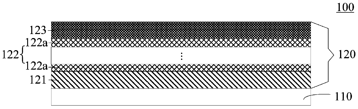
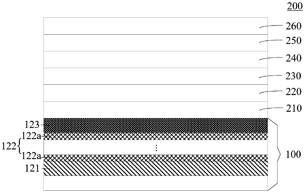
[0032] figure 1 is a schematic structural diagram of an AlN template provided by an embodiment of the present invention, such as figure 1 As shown, the AlN template 100 includes a substrate 110 and an AlN thin film 120 deposited on the substrate 110 .

[0033] The AlN thin film 120 includes a first AlN thin film 121, an insertion layer 122, and a second AlN thin film 123 stacked in sequence. The insertion layer 122 includes a plurality of AlNO sublayers 122a, and the oxygen content in the plurality of AlNO sublayers 122a is along the The stacking direction of the layers 122a first increases layer by layer and then decreases layer by layer.

[0034] In the embodiment of the present invention, the AlN thin film is set to include a firs...


PUM

PropertyMeasurementUnit
thicknessaaaaaaaaaa
thicknessaaaaaaaaaa
thicknessaaaaaaaaaa

Abstract

The invention discloses an AlN template, a light-emitting diode epitaxial wafer and a production method thereof and belongs to the field of semiconductor technologies. The AlN template comprises a substrate and an AlN thin film deposited on the substrate, wherein the AlN thin film comprises a first AlN thin film part, an inserted layer and a second AlN thin film part which are sequentially stacked, the inserted layer comprises multiple AlNO sub-layers, and oxygen content in the multiple AlNO sub-layers is increased layer by layer and then decreased layer by layer along the stacking direction of the multiple AlNO sub-layers. A part of O atoms in the AlNO sub-layers can replace N atoms, the other part of O atoms can form gap-filling atoms, both the replacing O atoms and the gap-filling O atoms can make AlN lattices distort to a certain extent, therefore, the lattice constant of the AlN thin film is increased, the lattice constant of the AlN thin film is more approximate to the lattice constant of a subsequent GaN epitaxial thin film, pressing stress in a GaN material can be reduced beneficially, warping of the epitaxial wafer is relieved, and then wavelength uniformity of an epitaxial layer is improved.

Description

technical field [0001] The invention relates to the technical field of semiconductors, in particular to an AlN template, a light-emitting diode epitaxial wafer and a manufacturing method thereof. Background technique [0002] LED (Light Emitting Diode, Light Emitting Diode) is a semiconductor electronic component that can emit light. As an efficient, environmentally friendly and green new solid-state lighting source, it is being rapidly and widely used, such as traffic lights, car interior and exterior lights, urban landscape lighting, mobile phone backlights, etc. [0003] The epitaxial wafer is the main component of the LED, and the existing GaN-based LED epitaxial wafer includes a sapphire substrate and a GaN epitaxial layer grown on the sapphire substrate. Since there are lattice mismatch and thermal mismatch problems between sapphire and GaN materials, and there is only a small lattice mismatch between AlN materials, GaN materials and sapphire substrates, AlN is often ...

Claims


Application Information

Patent Timeline
Patent Type & Authority Applications(China)
IPC IPC(8): H01L33/12H01L33/00
Inventor 陶章峰张武斌程金连乔楠胡加辉李鹏
Owner HC SEMITEK ZHEJIANG CO LTD
Why Eureka
Try Eureka