Light-emitting diode epitaxy structure with hole energy adjustment layer

A technology of hole energy regulation and light-emitting diodes, which is applied in the direction of electrical components, circuits, semiconductor devices, etc., can solve the problems of low hole injection efficiency and low internal quantum efficiency, so as to improve hole injection efficiency and overcome hole injection. Low efficiency, effect of increasing hole energy

Active Publication Date: 2016-07-06
ZHIXIN SEMICON (HANGZHOU) CO LTD
View PDF4 Cites 2 Cited by
  • Summary
  • Abstract
  • Description
  • Claims
  • Application Information

AI Technical Summary

Problems solved by technology

[0003] The technical problem to be solved by the present invention is to provide a light-emitting diode epitaxial structure with a hole energy adjustment layer, which inserts a layer of P-type semiconductor material holes with a low potential barrier in the P-type semiconductor material transport layer of the LED epitaxial structure. The hole energy adjustment layer uses the polarization electric field to increase the hole energy to improve the hole injection efficiency, and does not increase the hole barrier, which overcomes the defects of low hole injection efficiency and low internal quantum efficiency in the prior art

Method used


Image

  • Light-emitting diode epitaxy structure with hole energy adjustment layer
  • Light-emitting diode epitaxy structure with hole energy adjustment layer
  • Light-emitting diode epitaxy structure with hole energy adjustment layer

Examples


Embodiment 1

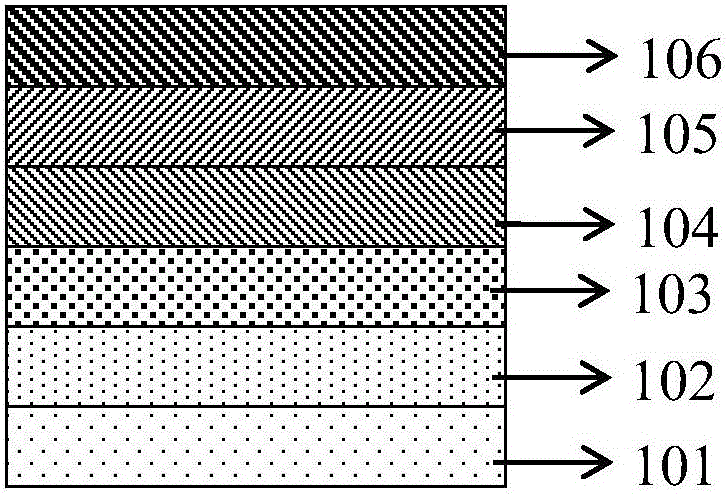
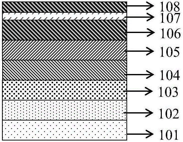
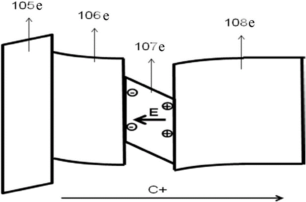
[0038] The light-emitting diode epitaxial structure with the hole energy adjustment layer in this embodiment includes a substrate 101, a semiconductor material buffer layer 102, an N-type semiconductor material 103, a multi-quantum well layer 104, and a P-type electron blocking layer from top to bottom. 105. P-type semiconductor material transport layer I 106, P-type semiconductor material hole energy adjustment layer 107 and P-type semiconductor material transport layer II 108, wherein the material of P-type semiconductor material hole energy adjustment layer 107 is Al 0.85 Ga 0.15 N, the thickness is 1nm, its lattice constant is larger than that of P-type semiconductor material transmission layer I106 and P-type semiconductor material transmission layer II108, and its band gap is smaller than that of P-type semiconductor material transmission layer I106 and P-type semiconductor material transmission layer II108.

[0039] Among the above, the substrate 101 is sapphire, and t...

Embodiment 2

[0050] The light-emitting diode epitaxial structure with the hole energy adjustment layer in this embodiment includes a substrate 101, a semiconductor material buffer layer 102, an N-type semiconductor material 103, a multi-quantum well layer 104, and a P-type electron blocking layer from top to bottom. 105. P-type semiconductor material transport layer I 106, P-type semiconductor material hole energy adjustment layer 107 and P-type semiconductor material transport layer II 108, wherein the material of P-type semiconductor material hole energy adjustment layer 107 is In 0.1 Ga 0.9 N, the thickness is 150nm, its lattice constant is larger than that of P-type semiconductor material transmission layer I106 and P-type semiconductor material transmission layer II108, and its band gap is smaller than that of P-type semiconductor material transmission layer I106 and P-type semiconductor material transmission layer II108.

[0051] Among the above, the substrate 101 is Si, and the sub...

Embodiment 3

[0062] The light-emitting diode epitaxial structure with the hole energy adjustment layer in this embodiment includes a substrate 101, a semiconductor material buffer layer 102, an N-type semiconductor material 103, a multi-quantum well layer 104, and a P-type electron blocking layer from top to bottom. 105. P-type semiconductor material transport layer I 106, P-type semiconductor material hole energy adjustment layer 107 and P-type semiconductor material transport layer II 108, wherein the material of P-type semiconductor material hole energy adjustment layer 107 is InN, The thickness is 300nm, its lattice constant is larger than that of P-type semiconductor material transport layer I106 and P-type semiconductor material transport layer II108, and its band gap is smaller than that of P-type semiconductor material transport layer I106 and P-type semiconductor material transport layer II108.

[0063] Among the above, the substrate 101 is SiC, and the substrate 101 is polar; the ...


PUM


Abstract

The invention provides a light-emitting diode epitaxy structure with a hole energy adjustment layer, and relates to a semiconductor device which has at least one potential jump barrier or surface barrier and is especially suitable for light emission. A P-type semiconductor material hole energy adjustment layer with a low barrier layer is inserted into a P-type semiconductor material transport layer of the LED epitaxy structure; the material is Al<x1>In<y1>Ga<1-x1-y1>N; in the formula, x1 is smaller than or equal to 1 and greater than or equal to 0; y1 is smaller than or equal to 1 and greater than or equal to 0; 1-x1-y1 is greater than or equal to 0; the thickness is 1-300nm; the lattice constant of the hole energy adjustment layer is greater than those of a P-type semiconductor material transport layer I and a P-type semiconductor material transport layer II; and the forbidden bandwidth is smaller than those of the P-type semiconductor material transport layer I and the P-type semiconductor material transport layer II. The hole energy is increased by a polarization electric field to improve the hole injection efficiency; a hole barrier is not increased; and the defects of low hole injection efficiency and low internal quantum efficiency in the prior art are overcome.

Description

technical field [0001] The technical solution of the invention relates to a semiconductor device specially suitable for light emission with at least one potential jump barrier or surface barrier, specifically a light emitting diode epitaxial structure with a hole energy adjustment layer. Background technique [0002] Semiconductor LED technology based on III-V nitrides has been widely used in the fields of display, lighting and backlighting. However, the problem of low hole injection efficiency of nitride LEDs has not been well resolved. This is mainly due to the fact that highly activated magnesium impurities make it difficult to obtain P-type nitride semiconductors with high hole concentrations, and the hole concentration of high-aluminum composition P-type nitride semiconductors in deep ultraviolet LEDs is particularly low, resulting in nitrogen Hole injection efficiency in compound LEDs is low. Heavy doping is a commonly used method to increase hole injection efficienc...

Claims


Application Information

Patent Timeline
Patent Type & Authority Applications(China)
IPC IPC(8): H01L33/02H01L33/32H01L33/14
CPCH01L33/02H01L33/14H01L33/32
Inventor 张紫辉张勇辉毕文刚徐庶耿翀
Owner ZHIXIN SEMICON (HANGZHOU) CO LTD
Why Eureka
Try Eureka