Method for forming field isolation

A field isolation and isolation layer technology, which is applied in the manufacturing of electrical components, circuits, semiconductor/solid-state devices, etc., can solve the problems of high cost, high process cost, and high manufacturing cost, and achieve low temperature, simple process steps, and high production cost. The effect of cost reduction

Inactive Publication Date: 2019-06-21
SHENZHEN UNIV
View PDF3 Cites 0 Cited by
  • Summary
  • Abstract
  • Description
  • Claims
  • Application Information

AI Technical Summary

Problems solved by technology

[0005] In addition, LOCOS must use SiO 2 For isolation, other oxides cannot be used as isolation materials, which also limits other applications; at the same time, LOCOS is a high-temperature technology, and the production cost is relatively high
[0006] The basic process of STI isolation technology is to deposit silicon nitride first, then etch a trench with a certain depth in the isolation area, then perform sidewall oxidation, and deposit SiO in the trench by CVD. 2 , and finally planarized by the CMP method to form trench isolation regions and active regions; the main problems are that the process cost is large and the operation is complicated
[0007] To sum up, both of the above two processes need to be carried out in a high temperature environment, the cost is high, and the isolation materials are all made of SiO 2 Mainly; and the two methods are mainly used for high-integration IC manufacturing. For applications that do not require high integration, such as display pixel applications and display drive circuit applications, the cost of the above-mentioned methods is too high and is not suitable for low-temperature manufacturing.

Method used


Image

  • Method for forming field isolation
  • Method for forming field isolation
  • Method for forming field isolation

Examples


Embodiment 1

[0039] In this embodiment, a Si sheet is selected as the substrate.

[0040] First, the substrate 1 is cleaned, and the cleaning process includes first using H 2 SO 4 and H 2 o 2 The mixed solution cleans the substrate, where H 2 SO 4 :H 2 o 2 =10:1, the temperature is set at 120°C, and the time is 10min; then the surface of the substrate 1 is rinsed with deionized water; and then cleaned with hydrofluoric acid solution, wherein HF:H 2 O=1:50, the temperature is set at 25°C, and the time is 1min; finally, rinse with deionized water. After the cleaning is completed, the surface of the substrate 1 is dried.

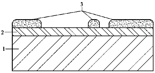
[0041] Reference attached figure 1 As shown, an isolation layer 2 with a thickness of 1 nm is grown on the surface of the substrate 1 after drying by the method of plasma enhanced chemical vapor deposition (Plasma Enhanced Chemical Vapor Deposition); in this embodiment, the isolation layer 2 for SiO 2 Floor.

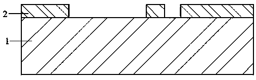
[0042] Reference attached figure 1 As shown, after ...

Embodiment 2

[0046] In this embodiment, a GaN sheet is selected as the substrate.

[0047] First, the substrate 1 is cleaned, and the cleaning process includes first using H 2 SO 4 and H 2 o 2 The mixed solution cleans the substrate, where H 2 SO 4 :H 2 o 2 =10:1, the temperature is set at 120°C, and the time is 10min; then the surface of the substrate 1 is rinsed with deionized water; and then cleaned with hydrofluoric acid solution, wherein HF:H 2 O=1:50, the temperature is set at 25°C, and the time is 1min; finally, rinse with deionized water. After the cleaning is completed, the surface of the substrate 1 is dried.

[0048] Reference attached figure 1 As shown, an isolation layer 2 with a thickness of 1mm is grown on the surface of the substrate 1 after drying by the method of low pressure chemical vapor deposition; in this embodiment, the isolation layer 2 is SiN x Floor.

[0049] Reference attached figure 1 As shown, after the isolation layer 2 is prepared on the substrat...

Embodiment 3

[0053] In this embodiment, a Si sheet is selected as the substrate.

[0054] First, the substrate 1 is cleaned, and the cleaning process includes first using H 2 SO 4 and H 2 o 2 The mixed solution cleans the substrate, where H 2 SO 4 :H 2 o 2 =10:1, the temperature is set at 120°C, and the time is 10min; then the surface of the substrate 1 is rinsed with deionized water; and then cleaned with hydrofluoric acid solution, wherein HF:H 2 O=1:50, the temperature is set at 25°C, and the time is 1min; finally, rinse with deionized water. After the cleaning is completed, the surface of the substrate 1 is dried.

[0055] Reference attached figure 1 As shown, an isolation layer 2 with a thickness of 1 mm is deposited on the surface of the substrate 1 after drying by a precipitation method; in this embodiment, the isolation layer 2 is Al 2 o 3 Floor.

[0056] Reference attached figure 1 As shown, after the isolation layer 2 is prepared on the substrate 1, the photoresist l...


PUM


Abstract

The invention relates to the technical field of electronic devices and integrated circuit technology and relates to a method for forming field isolation. The method comprises the steps of preparing anisolation layer, wherein the isolation layer is prepared on the surface of a substrate through a thin film growth method or a precipitation method after the substrate is cleaned and dried; determining a trench of an active area, and marking the position of the trench of the active area on the isolation layer through a photoetching method; etching the trench of the active area, and removing the isolation layer covered on the position of the trench of the active area through an etching method in the position of the trench of the active area, wherein the thickness of the isolation layer is 1 nm-1 mm. According to the method in the invention, low temperature and low cost of production and processing of integrated boards can be realized, and industrialization is facilitated.

Description

technical field [0001] The invention belongs to the technical field of electronic devices and integrated circuits, and relates to a method for forming field isolation. Background technique [0002] The complete circuit is connected by separate devices through specific electrical pathways, so the devices must be able to be isolated in the manufacture of integrated circuits, and these devices must then be able to be interconnected to form the required specific circuit structure; if Poor isolation will cause leakage, low breakdown, latch-up effect, etc.; therefore, isolation technology is a key technology in integrated circuit manufacturing. Today, there are two main isolation technologies: local oxidation (LOCOS: Local Oxidation of Silicon) isolation technology and shallow trench isolation (STI: Shallow Trench Isolation) isolation technology. [0003] The manufacturing process of the LOCOS structure is to use the characteristics of the SiN film to mask the oxide layer. First,...

Claims


Application Information

Patent Timeline
Patent Type & Authority Applications(China)
IPC IPC(8): H01L21/02
Inventor 张猛闫岩周玮李贵君郭海成
Owner SHENZHEN UNIV
Why Eureka
Try Eureka