Spin wave logic device based on Bloch-type domain wall

A logic device and spin wave technology, applied in waveguide-type devices, logic circuits with logic functions, instruments, etc., can solve the problem of difficult to apply magnon system, low spin wave transmission speed, and difficult to design high transmission speed and other issues, to achieve the effect of easy miniaturization, small manufacturing process, and reduced energy consumption

Active Publication Date: 2019-07-02
UNIV OF ELECTRONICS SCI & TECH OF CHINA
View PDF4 Cites 5 Cited by
  • Summary
  • Abstract
  • Description
  • Claims
  • Application Information

AI Technical Summary

Problems solved by technology

However, this kind of waveguide is mainly based on the structure of Neel-type domain walls, and the spin waves transmitted by it have non-reciprocity, that is, at the same excitation frequency, the spin waves propagate along the positive and negative directions of the domain walls with Different amplitudes and speeds make it difficult to apply it to magnon systems and make devices with logic functions
In addition, its spin wave transmission speed is low, it is difficult to design devices with high transmission rate function

Method used


Image

  • Spin wave logic device based on Bloch-type domain wall
  • Spin wave logic device based on Bloch-type domain wall
  • Spin wave logic device based on Bloch-type domain wall

Examples


Embodiment

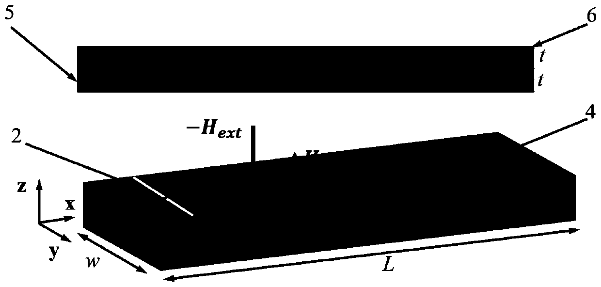
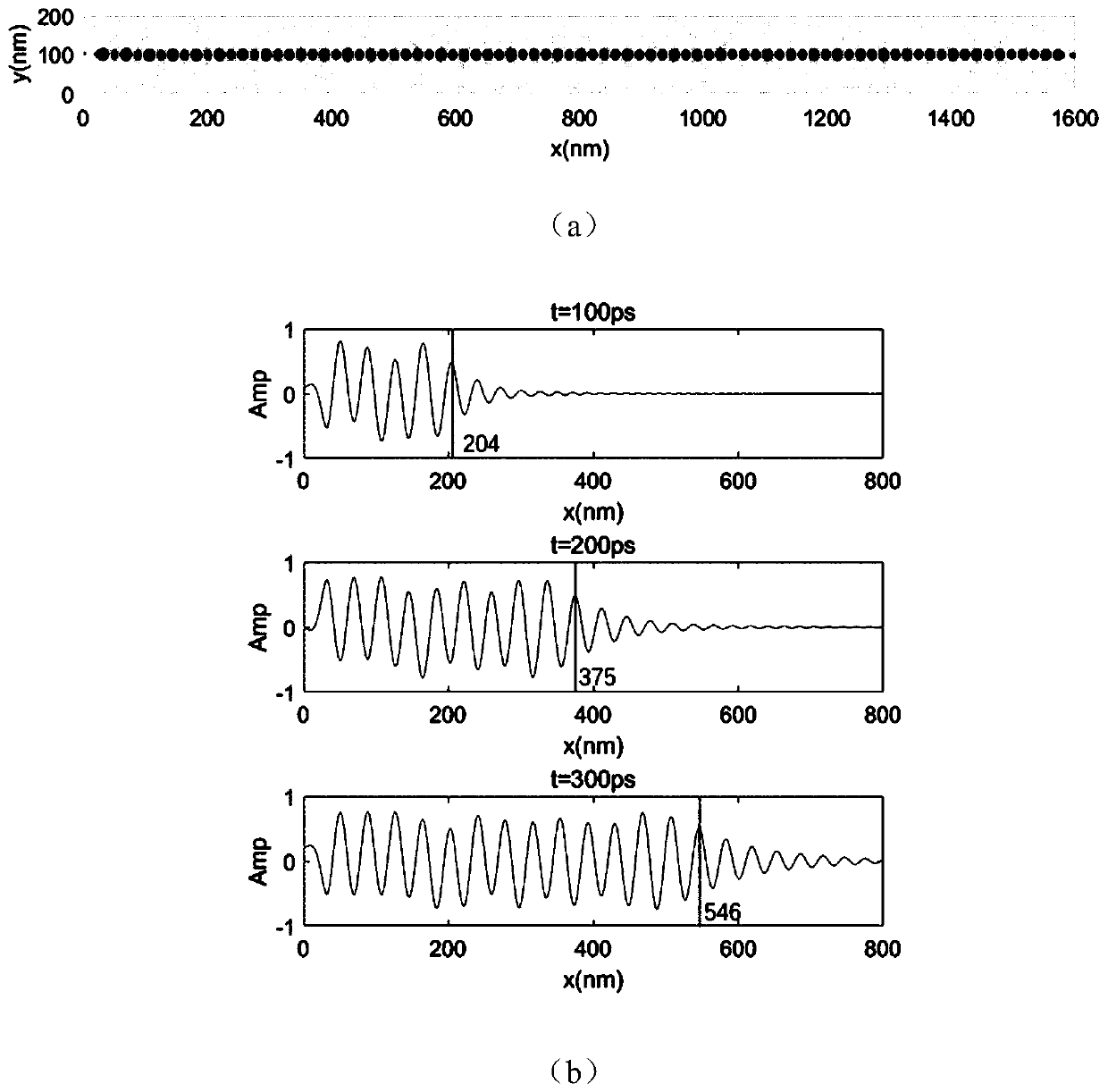
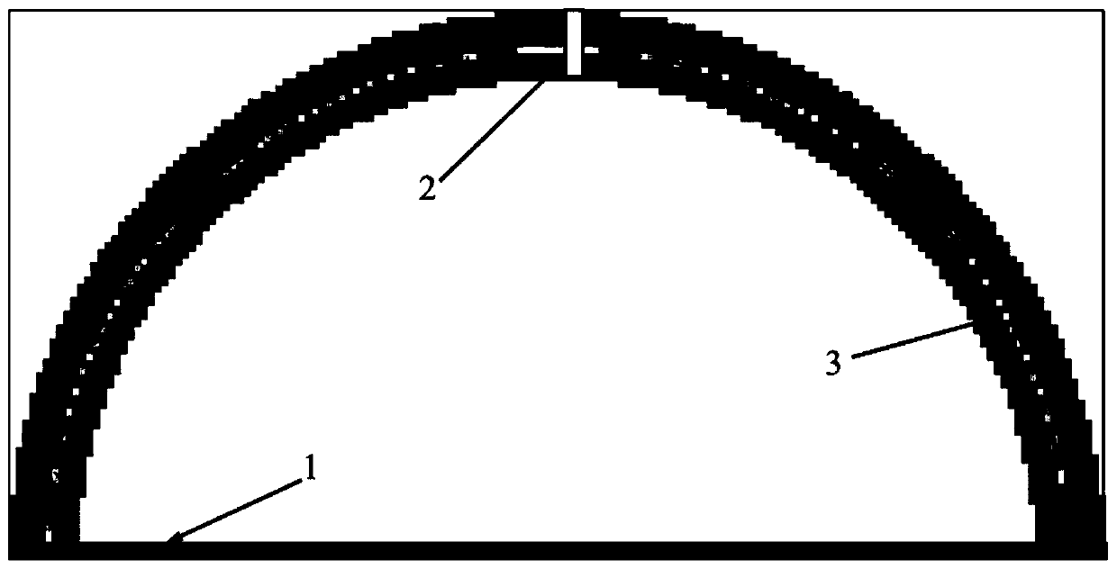
[0041] In the embodiment, the dimensions of the hard magnetic layer and the soft magnetic layer of the strip waveguide are: length L=1 μm, width w=200nm, thickness t=2nm; the inner diameter of the arc-shaped curved waveguide outer diameter Thickness t = 2 nm. Use a magnetic head to apply an external magnetic field H vertical to the surface of the film and vertical to the area on both sides of the film surface, respectively. ext , the magnitude of the external field is 1T and decays exponentially with time, and finally the waveguide obtains a stable Bloch-type domain wall structure. Subsequently, image 3 A 25GHz sinusoidal micromagnetic signal is applied to the position of the medium microstrip antenna, the direction is perpendicular to the surface of the soft magnetic layer film, and the amplitude is 0.1T. Such as Figure 4 In the above, applying a bias magnetic field in the box area represents the input signal 1, and no bias field represents the input signal 0, resultin...


PUM


Abstract

The invention discloses a spin wave logic device based on a Bloch type domain wall, and belongs to the technical field of magnetic oscillator devices. The spin wave logic device comprises a bent domain wall waveguide, a microstrip antenna for exciting spin waves and a receiving antenna, wherein the bent domain wall waveguide comprises a hard magnetic layer and a soft magnetic layer positioned on the hard magnetic layer, the microstrip antenna for exciting spin waves is fixedly connected with two ends of the bent domain wall waveguide, and the receiving antenna is positioned on a symmetry axisof the bent domain wall waveguide and is fixedly connected with the soft magnetic layer of the bent domain wall waveguide. According to the spin wave logic device provided by the invention, the spin wave transmission is based on the Bloach-type domain wall waveguide, and the hard magnetic layer has an influence on the effective field distribution of the soft magnetic layer through an exchange coupling effect, so that the soft magnetic layer forms a nano-scale Bloach-type domain wall. Therefore, external field energy input is not needed during spin wave transmission, the energy consumption of the system is greatly reduced, and meanwhile, the anti-interference performance of spin waves is enhanced.

Description

technical field [0001] The invention belongs to the technical field of magnon devices, and in particular relates to a spin wave logic device based on a Bloch-type domain wall controlled by a magnetic field. Background technique [0002] Traditional CMOS devices use carriers to transmit and process information, but with the miniaturization of devices, their performance is close to the physical limit, because in the high-frequency, low-scale environment, its manufacturing technology, production cost and High power consumption during operation limits its future development. Therefore, the development of new ultra-CMOS devices, that is, "non-charge devices" will be the only way for the development of integrated circuits in the future. As an alternative approach, the development of magnon devices holds great potential and advantages. Magnon is the quantum state of spin wave, which is generated by the resonance excitation of ordered magnetic materials. It can be applied to signa...

Claims


Application Information

Patent Timeline
Patent Type & Authority Applications(China)
IPC IPC(8): H03K19/20H01P3/00G06F17/50
CPCH03K19/20H01P3/00G06F30/367
Inventor 钟智勇高雷森刘爽金立川廖宇龙文天龙唐晓莉张怀武
Owner UNIV OF ELECTRONICS SCI & TECH OF CHINA
Why Eureka
Try Eureka