Wafer dopant image segmentation method, system, computer equipment and storage medium

A technology of image segmentation and doping, applied in image analysis, calculation, image enhancement, etc., can solve the problem of low density, achieve the effect of improving segmentation accuracy, high robustness, and image segmentation accuracy

Active Publication Date: 2020-11-24
SOUTH CHINA UNIV OF TECH
View PDF3 Cites 0 Cited by
  • Summary
  • Abstract
  • Description
  • Claims
  • Application Information

AI Technical Summary

Problems solved by technology

And the oxide layer on the highly doped silicon surface is less dense than the oxide layer grown on other layers

Method used


Image

  • Wafer dopant image segmentation method, system, computer equipment and storage medium
  • Wafer dopant image segmentation method, system, computer equipment and storage medium
  • Wafer dopant image segmentation method, system, computer equipment and storage medium

Examples


Embodiment 1

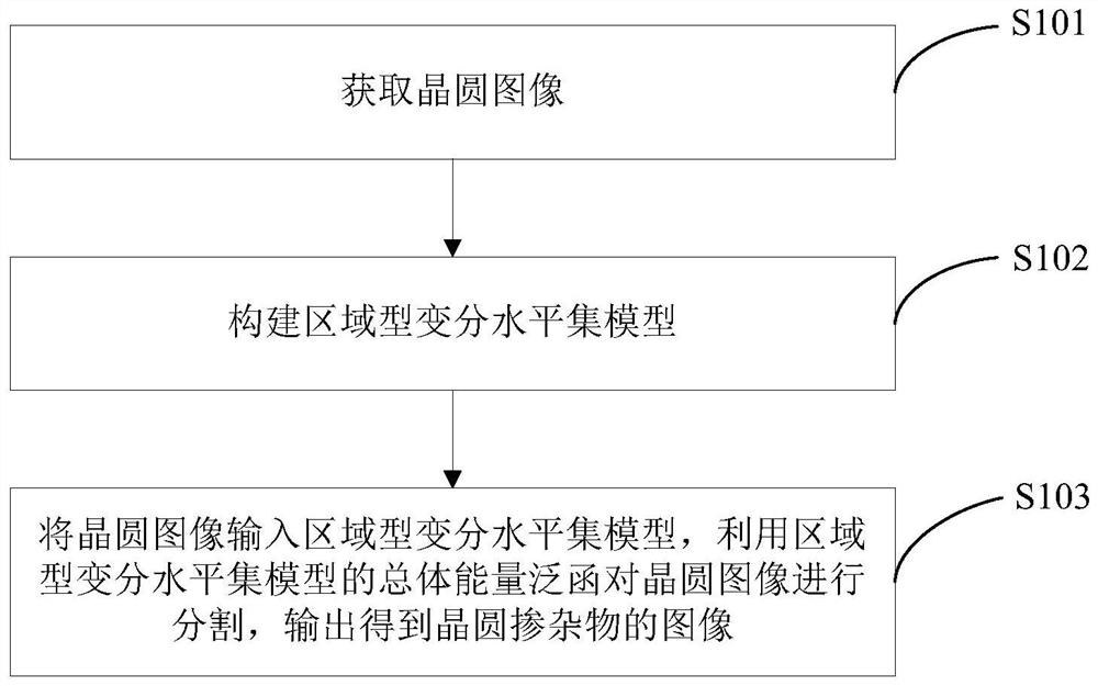
[0068] Such as figure 1 As shown, the present embodiment provides a method for image segmentation of wafer dopant, the method comprising the following steps:

[0069] S101. Obtain a wafer image.

[0070] In this embodiment, the wafer image is obtained by zooming in and collecting with a metallographic microscope. According to the color depth of the dopant in the wafer image is different, and the gray scale of the wafer image is uneven and affected by noise, it needs to be segmented.

[0071] S102. Construct a regional variational level set model.

[0072] The overall energy functional of the regional variational level set model is as follows:

[0073]

[0074] Among them, Ω represents the image space; φ(x, y) represents the level set function, and the signed distance function is generally used; u 0 (x,y) represents the image pixel;

[0075] Indicates the smoothing term of the evolution curve, which makes the zero level set as short and smooth as possible, u 1 Indicat...

Embodiment 2

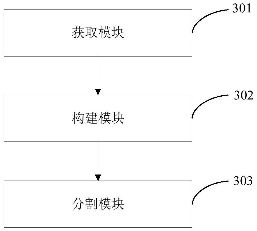
[0109] Such as image 3 As shown, the present embodiment provides a system for image segmentation of wafer dopant, the system includes an acquisition module 301, a construction module 302 and a segmentation module 303, and the specific functions of each module are as follows:

[0110] The acquiring module 301 is configured to acquire wafer images.

[0111] The construction module 302 constructs a regional variational level set model.

[0112] The segmentation module 303 is configured to input the wafer image into the regional variational level set model, segment the wafer image using the overall energy functional of the regional variational level set model, and output the image of the wafer dopant .

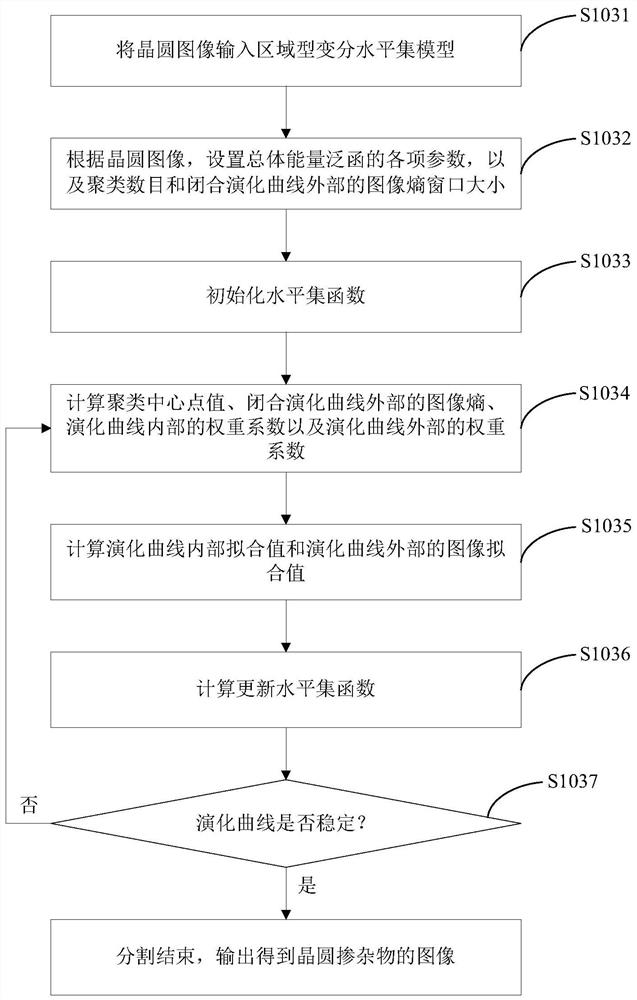
[0113] Further, segmentation module 303 such as Figure 4 shown, including:

[0114] The input unit 3031 is used for inputting the wafer image into the regional variational level set model.

[0115] The setting unit 3032 is configured to set various parameters of the overall...

Embodiment 3

[0124] This embodiment provides a computer device, which may be an industrial computer in an image acquisition device, and the structure of the industrial computer is as follows: Figure 5 As shown, it includes a processor 502 connected through a system bus 501, a memory, an input device 503, a display 504, and a network interface 505. The processor is used to provide computing and control capabilities. The memory includes a non-volatile storage medium 506 and internal Memory 507, the non-volatile storage medium 506 stores an operating system, computer programs and databases, the internal memory 507 provides an environment for the operation of the operating system and computer programs in the non-volatile storage medium, and the processor 502 executes memory storage During computer program, realize the image segmentation method of above-mentioned embodiment 1, as follows:

[0125] Get the wafer image;

[0126] Build regional variational level set models;

[0127] The wafer i...


PUM


Abstract

Disclosed in the present invention are an image segmentation method and system for a wafer dopant, a computer device, and a storage medium. The method comprises: obtaining a wafer image; constructing a regional variational level set model; and inputting the wafer image into the regional variational level set model, segmenting the wafer image by using the total energy functional of the regional variational level set model, and outputting an image of a wafer dopant. The system comprises an obtaining module, a construction module, and a segmentation module. According to the present invention, a wafer image affected by noise is input into a constructed regional variational level set model and the wafer image is then segmented by using the total energy functional of the regional variational level set model, so that a wafer dopant can be accurately segmented from the wafer image, and the segmentation precision for an image having a low contrast ratio can be improved.

Description

technical field [0001] The invention relates to an image segmentation method, system, computer equipment and storage medium of a wafer dopant, and belongs to the technical field of image segmentation. Background technique [0002] Wafers are the basic material for manufacturing semiconductor chips. Various circuit element structures can be processed on the wafer, and become IC products with specific electrical functions. According to the excellent performance of SiC, GaN, and ZnO material devices, the third-generation semiconductors are rapidly emerging, especially nitride materials, which have large band gaps (the forbidden band is usually above 2eV), high breakdown electric fields, and high electron saturation. Drift speed, strong anti-irradiation ability and other advantages solve the problem of white light lighting, and are suitable for the development of high temperature, high power devices and various electronic devices working in special environments. [0003] The w...

Claims


Application Information

Patent Timeline
Patent Type & Authority Patents(China)
IPC IPC(8): G06T7/00G06T7/11
CPCG06T7/0008G06T7/11G06T2207/30148
Inventor 胡跃明黄丹李璐
Owner SOUTH CHINA UNIV OF TECH
Why Eureka
Try Eureka