Preparation method of light-emitting device

A technology for light-emitting devices and pixel-defining layers, which is applied in the manufacturing of semiconductor/solid-state devices, electric solid-state devices, semiconductor devices, etc., can solve the problem that the pixel-defining layer is difficult to meet the requirements of the preparation process of full-color light-emitting devices, and achieve easy pixel uniformity. , The effect of preventing electrode short circuit and avoiding open circuit

Active Publication Date: 2019-07-09
SHENZHEN TCL IND RES INST
View PDF6 Cites 1 Cited by
  • Summary
  • Abstract
  • Description
  • Claims
  • Application Information

AI Technical Summary

Problems solved by technology

[0005] In view of the deficiencies in the prior art above, the purpose of the present invention is to provide a method for manufacturing a light-emitting device, aiming at solving the problem that the existing pixel-defining layer with a single structure cannot meet the requirements of the manufacturing process of a full-color light-emitting device

Method used


Image

  • Preparation method of light-emitting device
  • Preparation method of light-emitting device
  • Preparation method of light-emitting device

Examples


Embodiment 1

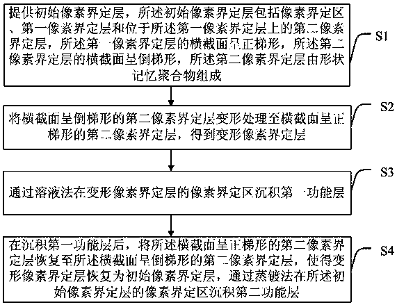
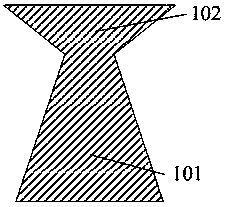
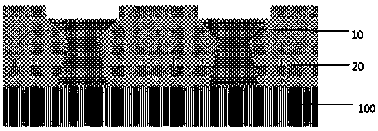
[0085] Add bisphenol A cyanate to the flask, heat to 100 degrees Celsius, and after it is completely melted, add polyethylene glycol, where the mass ratio of bisphenol A cyanate to polyethylene glycol is 10:1, stir and mix After being uniform, put it in a vacuum drying oven at 100-110 degrees Celsius and bake for 0.5-1 h, and then pour the mixture into the hourglass-shaped first mold 20 placed on the substrate 100, such as image 3 As shown, heating at 120-130 degrees Celsius for 2 to 3 hours for curing, and then heating at 210-230 degrees Celsius for 5 hours for post-curing. The hourglass-shaped first mold is removed to obtain an initial pixel defining layer with shape memory. Its glass The transformation temperature is 260~270 degrees Celsius;

[0086] The initial pixel delimiting layer is heated to a temperature T of 280~300 degrees Celsius, and the second mold 30 is used to maintain a uniform pressure F to make the initial pixel delimiting layer reach a preset deformation amou...

Embodiment 2

[0089] Preheat epoxy resin E-51 and methyl tetrahydrophthalic anhydride to 60 degrees Celsius respectively, mix and stir evenly, add 2-ethyl-4-methylimidazole, epoxy resin E-51, methyl The mass ratio of tetrahydrophthalic anhydride and 2-ethyl-4-methylimidazole is 100:60:1. After mixing and stirring evenly, put the resin system in an oven at 80 degrees Celsius and let it stand still, until the bubbles are removed ; Then the mixture is poured into the first hourglass mold 20 placed on the substrate 100, such as image 3 , And then heat at 80-90 degrees Celsius for 2 to 3 hours, 100 degrees Celsius for 2 hours, and 150 degrees Celsius for 2 hours, and then remove the first mold to obtain the initial pixel defining layer with a glass transition temperature of 70 to 90 degrees Celsius;

[0090] The initial pixel defining layer is heated to a temperature T of 100~120 degrees Celsius, and the second mold 30 is used to maintain a uniform pressure F to make the initial state shape memory ...

Embodiment 3

[0093] Mix polyethylene adipate glycol ester glycol (PEA), 1,4-butanediol (BD) and diphenylamine (DPA) according to the mass ratio of PEA, BD, and DPA to 5:4:3 and then heat to 100 ~120 degrees Celsius, dehydrated under vacuum until the water content is less than 0.02%; then under room temperature nitrogen environment, add a metered amount of 4,4-diphenylmethane diisocyanate (MDI), the mass ratio of MDI to the previously added BD is 2: Add the amount of 1, and then quickly stir evenly, and then pour the mixed mixture into the hourglass-shaped first mold 20 placed on the substrate 100, such as image 3 , Cured at room temperature for 3 hours, put it in an oven for curing at 80 degrees Celsius for 24 hours, after removing the hourglass mold, the initial pixel defining layer in the initial state is obtained, and the glass transition temperature is 60 to 70 degrees Celsius;

[0094] The initial state of the pixel defining layer is heated to a temperature T of 80 to 100 degrees Celsius...


PUM


Abstract

The invention discloses a preparation method of a light-emitting device, including the steps of providing an initial pixel defining layer, comprising pixel defining areas, a first pixel defining layerand a second pixel defining layer on the first pixel defining layer, wherein the cross section of the first pixel defining layer is in the shape of an upright trapezoid, the cross section of the second pixel defining layer is in the shape of an inverted trapezoid, and the second pixel defining layer is composed of shape memory polymers; transforming the second pixel defining layer with inverted trapezoidal cross section into a second pixel defining layer with upright trapezoidal cross section, so as to obtain a transformed pixel defining layer; depositing a first functional layer in the pixeldefining area of the transformed pixel defining layer through a solution method; and after deposition of the first functional layer, recovering the second pixel defining layer with upright trapezoidal cross section into the second pixel defining layer with inverted trapezoidal cross section so as to recover the transformed pixel defining layer into the initial pixel defining layer, and depositinga second functional layer in the pixel defining area of the initial pixel defining layer by means of evaporation.

Description

Technical field [0001] The present invention relates to the technical field of light-emitting devices, in particular to a method for preparing a light-emitting device. Background technique [0002] Quantum dots have many advantages such as easy adjustment of luminous color, high color saturation, solution processability, high stability, etc., making quantum dot light-emitting diodes (QLEDs) regarded as a strong competitor of next-generation display technology. Quantum dot light-emitting diodes usually adopt a multilayer structure, so that in the actual manufacturing process of QLEDs, two or more thin film preparation methods are often used at the same time. For example, in positive quantum dot devices, thin films are deposited sequentially in the order of anode, hole injection layer, hole transport layer, quantum dot light-emitting layer, electron transport layer, and cathode, usually on the anode-plated substrate. To deposit the light-emitting functional layer and the cathode, ...

Claims


Application Information

Patent Timeline
Patent Type & Authority Applications(China)
IPC IPC(8): H01L51/56H01L27/32H01L51/00
CPCH10K59/122H10K71/164H10K71/12H10K71/00
Inventor 张滔向超宇李乐辛征航王雄志
Owner SHENZHEN TCL IND RES INST
Why Eureka
Try Eureka