Method for detecting focus variation between wafer center and wafer edge and compensation method thereof
A compensation method and technology of variation, applied in the field of integrated circuit manufacturing, can solve the problems of inconsistent wafer thickness, out of focus, affecting product yield, etc., and achieve the effect of improving wafer yield
- Summary
- Abstract
- Description
- Claims
- Application Information
AI Technical Summary
Problems solved by technology
Method used
Image

Examples
Embodiment Construction
[0026] The technical solutions in the present invention will be clearly and completely described below in conjunction with the accompanying drawings. Apparently, the described embodiments are part of the embodiments of the present invention, not all of them. Based on the embodiments of the present invention, all other embodiments obtained by persons of ordinary skill in the art without making creative efforts belong to the protection scope of the present invention.
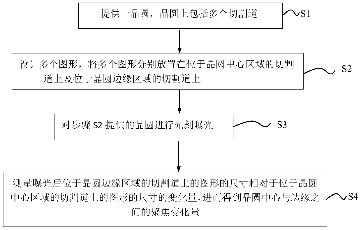
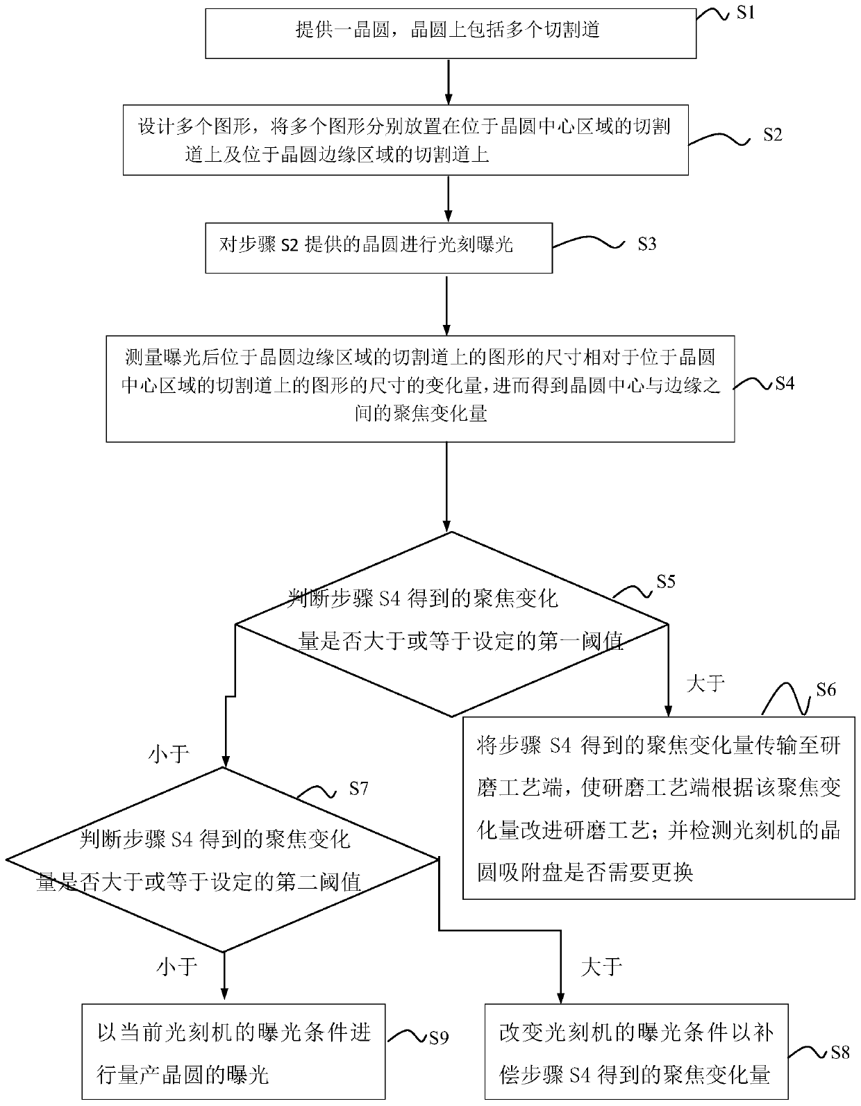
[0027] In one embodiment of the present invention, a method for detecting the amount of focus variation between the center and the edge of the wafer is provided. The method includes: S1: providing a wafer with a plurality of dicing lines; S2: designing multiple A plurality of graphics are respectively placed on the dicing line located in the central area of the wafer and on the dicing line located in the edge area of the wafer; S3: performing photolithography exposure to the wafer provided in step S2; S4: measu...
PUM
 Abstract
Description
Claims
Application Information
 - R&D
- Intellectual Property
- Life Sciences
- Materials
- Tech Scout
- Unparalleled Data Quality
- Higher Quality Content
- 60% Fewer Hallucinations
Browse by: Latest US Patents, China's latest patents, Technical Efficacy Thesaurus, Application Domain, Technology Topic, Popular Technical Reports.
© 2025 PatSnap. All rights reserved.Legal|Privacy policy|Modern Slavery Act Transparency Statement|Sitemap|About US| Contact US: help@patsnap.com