Semiconductor device and method of forming the same

A semiconductor and device technology, applied in the field of semiconductor devices and their formation, can solve the problems of reducing the concentration gradient of TFET LDD junction, device tunneling probability and on-state current reduction, TFET tunneling probability and driving current, etc. Transit probability and drive current, reduce thermal budget, increase the effect of concentration gradient

Active Publication Date: 2021-01-05
SEMICON MFG INT (SHANGHAI) CORP +1
View PDF8 Cites 0 Cited by
  • Summary
  • Abstract
  • Description
  • Claims
  • Application Information

AI Technical Summary

Problems solved by technology

[0004] In the existing TFET manufacturing process, TFET lightly doped drain (Lightly Doped Drain, LDD) process and CMOS LDD process are carried out before the LDD annealing (Anneal) process, for example, ion implantation process is used before or after the CMOS LDD process TFET LDD is formed, so the dopant ions of TFET LDD will undergo LDD Anneal and the source / drain anneal (Source / Drain Anneal) after the source-drain doped region is formed, because the high temperature in the annealing process will affect the heat of the dopant ions of TFET LDD budget, and reduce the concentration gradient of the TFET LDD junction, which will easily lead to a decrease in the TFET tunneling probability and drive current, and a decrease in the device tunneling probability and on-state current

Method used


Image

  • Semiconductor device and method of forming the same
  • Semiconductor device and method of forming the same
  • Semiconductor device and method of forming the same

Examples


Embodiment Construction

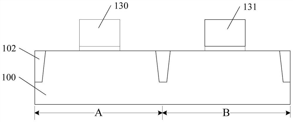
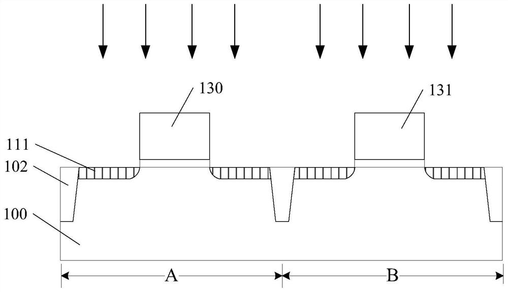
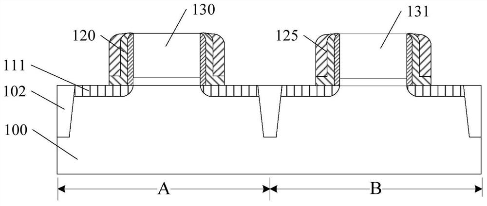
[0029] As mentioned in the background technology, in the existing TFET manufacturing process, both the TFET lightly doped drain process and the CMOS lightly doped drain process are performed before the LDD annealing process, for example, before the CMOS lightly doped drain process Or use the ion implantation process to form the TFET lightly doped drain region afterwards, so the dopant ions in the TFET lightly doped drain region will experience LDD Anneal and Source / Drain Anneal after forming the source and drain doped regions, because the high temperature in the annealing process will Affecting the thermal budget of the dopant ions in the lightly doped drain region of the TFET, and reducing the concentration gradient of the lightly doped drain region junction of the TFET, will easily lead to a decrease in the tunneling probability and driving current of the TFET, and a decrease in the tunneling probability and on-state current of the device.

[0030] Figure 1 to Figure 4 It is...


PUM


Abstract

The invention discloses a semiconductor device and a forming method thereof, and the method comprises the steps: providing a semiconductor substrate which comprises a TFET region and a CMOS region; covering the TFET region by adopting a first covering layer, forming a CMOS lightly-doped drain region in the CMOS region under the protection of the first covering layer, and carrying out first annealing process treatment; removing the first covering layer, and forming a TFET grid side wall and a CMOS grid side wall; forming a source-drain doped region in the TFET region and the CMOS region, and carrying out second annealing process treatment; forming a protective layer covering the CMOS region, removing at least one part of the side wall of the TFET gate under the protection of the protectivelayer, and exposing the semiconductor substrate between the TFET gate and the source-drain doped region of the TFET region; and forming a TFET lightly-doped drain region in the TFET region. Accordingto the scheme, the concentration gradient of the junction surface of the lightly-doped drain region of the TFET can be improved, and the tunneling probability and the on-state current of the device are improved.

Description

technical field [0001] The invention relates to the technical field of semiconductor manufacturing, in particular to a semiconductor device and a forming method thereof. Background technique [0002] With the development of semiconductor technology, negative effects such as the short channel effect of devices are becoming more and more serious. The impact of the short channel effect can be reduced by replacing a traditional Metal-Oxide-Semiconductor Field-Effect Transistor (MOSFET) with a Tunneling Field-effect Transistor (TFET). Due to the excellent sub-threshold characteristics of TFET, the operating voltage can be greatly reduced compared with CMOS, so it is suitable for the field of ultra-low leakage and ultra-low power consumption. Unlike conventional CMOS, the source and drain regions of a TFET are doped differently. [0003] In circuit design, TFETs often need to be matched with standard CMOS devices, so the TFET process and the CMOS process are often set to be comp...

Claims


Application Information

Patent Timeline
Patent Type & Authority Patents(China)
IPC IPC(8): H01L21/8232H01L21/8238H01L27/088H01L27/092
CPCH01L21/8232H01L21/8238H01L21/823892H01L27/088H01L27/0922
Inventor 王文博唐粕人卜伟海宁先捷
Owner SEMICON MFG INT (SHANGHAI) CORP
Why Eureka
Try Eureka